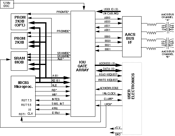
Fig. 1.1 IOU GA as a block of the RT-IOU AACS
An ASIC specification should create an unambiguous description of an ASIC device that guides the ASIC designer's development work, the ASIC vendor's manufacturing, test and screening work, and the system implementor's work. With this description, which may exist at many levels, the manager of an ASIC program can measure the technical progress of the ASIC design and provide support for contracting and procuring the ASIC parts. In this appendix, we examine a case study of a technical specification. Please see the "ASIC Design" section: Chapter 1 for a description of a generic technical specification of an ASIC.
Along with conventional paper-based documentation, modern ASIC design produces a significant amount of computer-based information. This may include a high-level language behavioral description, a gate-level circuit net list, files of test patterns, schematic images, etc. No ASIC specification is complete without a comprehensive listing and configuration management of these files and their various revisions.
Based around an actual part specification, we intend this appendix not to deliver a "fill-in-the-blanks" template but to show all major areas requiring technical specification. Studying this appendix will provide you with the kind of information essential to support the activities discussed in the first paragraph above. The example ASIC we chose comes from the NASA Cassini spacecraft.
The spacecraft's mission is to orbit the planet Saturn in the late 1990s and gather scientific data. Upon arrival in the Saturn system, the spacecraft will launch a probe to the Saturnian moon, Triton, where, among other experiments, it will explore Triton's unusual carbon chemistry.
The ASIC itself is known as the Attitude and Articulation Control Subsystem Remote Terminal Input/Output Unit or IOU, for short. As part of the control and data interface, the IOU supports the spacecraft subsystem responsible for steering and dynamic configuration control.
The following are actual pages from a specification. We have added brief comments. The comments are separated from the pages by horizontal divisions such as the one below.
This first page below shows the IOU gate array table of contents. The following gives a brief introduction to each major section of the technical specification.
TABLE OF CONTENTS
Scope....................................................5
Applicable Documents.....................................5
Conventions Used.........................................5
Additional Requirements..................................6
1. Chip Overview........................................7
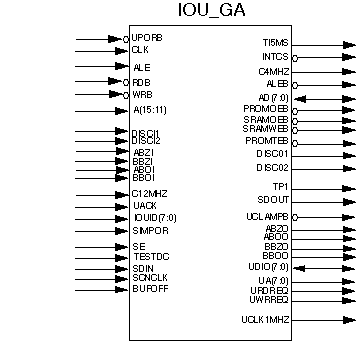
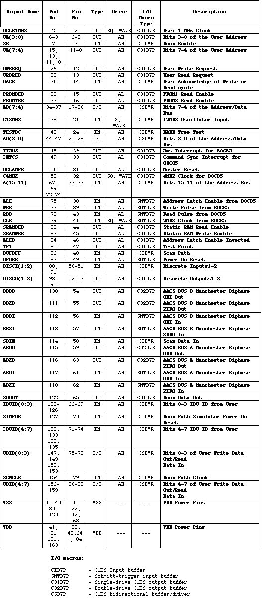
2. IOU ASIC Signal Designations and Descriptions........11
3. Functional Description...............................14
3.1 IOU Gate Array Timing Chain........................15
3.2 IOU Gate Array Address Decoder.....................15
3.3 IOU Gate Array Memory Control......................15
3.4 IOU Gate Array Manchester Encoder/Decoder..........16
3.5 IOU Gate Array Bus Select & AACS Bus I/F...........16
3.6 IOU Gate Array User I/F............................16
3.7 IOU Gate Array Discrete I/O........................17
3.8 Worst case timing specifications and diagrams......18
4. Testability Constructs...............................30
4.1 Use of Scan.......................................30
4.2 NAND tree for DC tests............................30
5. Electrical Characteristics...........................31
5.1 Electrical Test Requirements......................31
5.2 Absolute Maximum Ratings..........................32
5.3 Recommended Operating Conditions..................33
5.4 DC Characteristics................................34
5.4.1 DC Electrical Performance Characteristics.....34
5.4.2 IDDQ Testing..................................36
5.4.3 Pulldown Resistors............................36
5.4.4 Pullup Resistors..............................36
5.5 AC Characteristics................................37
5.5.1 AC Electrical Performance Characteristics.....37
5.5.2 Timing Analysis...............................38
5.5.2.1 Pre-Layout Timing Margins.................38
5.5.2.2 Post-Layout Timing Margins................38
5.5.2.3 Tester Specification Limits...............38
5.5.3 Tester Load Circuit...........................39
5.6 Burn-In...........................................40
5.6.1 Static Burn-In................................40
5.6.2 Dynamic Burn-In...............................40
5.6.3 Burn-In Configuration.........................41
5.6.4 Delta Limits..................................43
6. Physical Characteristics.............................44
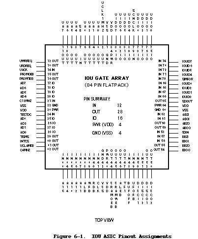
6.1 Pin Assignment....................................44
6.2 Bonding Diagram...................................45
6.3 Package Outline...................................47
6.4 Marking Diagram...................................48
7. Device Statistics....................................49
8. Exceptions to CS515577B..............................50
This list of tables and figures gives a quick look at the design technical content of the spec.
LIST OF TABLES

Table 2-1.  Signal Description...............................12
Table 3-1.  IOU Memory Map...................................15
Table 3-2.  IOU GA Worst Case Timing Spec....................18
Table 5-1.  Electrical Test Requirements.....................31
Table 5-2.  Absolute Maximum Ratings.........................32
Table 5-3.  Recommended Operating Conditions.................33
Table 5-4.  DC Performance Characteristics...................34
Table 5-5.  AC Performance Characteristics...................37
Table 5-6.  Burn-In Connections..............................41
Table 5-7.  Delta Limits.....................................43
Table 6-1.  Connections Table................................46

LIST OF FIGURES

Figure 1-1.  IOU GA in RT Input/Output AACS..................8
Figure 1-2.  IOU GA Block Diagram............................9
Figure 1-3.  IOU GA Module Diagram...........................10
Figure 2-1.  IOU GA ASIC Symbol..............................11
Figure 3-1.  AACS RT IOU/USER IF Timing......................19
Figure 3-2.  Status Read Cycle...............................20
Figure 3-3.  Local Echo Enable Write Cycle...................20
Figure 3-4.  USERIF Write Cycle..............................21
Figure 3-5.  USERIF Read Cycle...............................22
Figure 3-6.  SRAM Write Cycle................................23
Figure 3-7.  SRAM Read Cycle.................................24
Figure 3-8.  PROM Read Cycle.................................25
Figure 3-9.  Zero Crossing Deviation +150 on Manchester......26
Figure 3-10. Status Word Read - Valid Word Manchester........27
Figure 3-11. Zero Crossing Deviation -150 on Word Manchester.28
Figure 3-12. Status Word Read - Valid Word Manchester........29
Figure 5-1.  Switching Test Circuit and Waveforms............39
Figure 6-1.  IOU GA Pinout Assignments.......................44
Figure 6-2.  Bonding Diagrams................................45
Figure 6-3.  Package Outline (84 pin Flatpack)...............47
Figure 6-4.  Marking Diagram.................................48
Scope
This document is a procurement specification for IOU Gate Array devices. It represents the functional specifications for the IOU Gate Array along with its electrical characteristics, physical characteristics, device level statistics and physical characteristics.
This document shall be the sole source of design and procurement specifications for the IOU Gate Array, and shall supersede any other specification documents issued prior to this release.
Applicable Documents
Primary sources of functional and environmental requirements for this device:
RTIOU (Remote Terminal IOU) Attitude and Articulation Control Subsystem Cassini Mission H/W Requirements
Conventions Used
All signals are active high unless designated with a "B": after a signal name. For example, "ALE" is active high and "WRB" is active low.
Additional requirements d and e have to do with JPL requirements for appropriate types of information format and tools.
a. Functional Delay Simulation: To be derived from each final application specific electrical design and electrical design and layout (i.e. post-routed design). Simulation shall be accomplished by using actual delays as computed from the placement and layout of the device as it will be fabricated. Actual delays shall include the contribution associated with the delay through the gate as well as the contribution due to actual metal capacitance and loading on the output(s). Using these actual delays, the application specific design shall insure the absence of timing violations in the circuit. Such timing violations shall include, but not limited to, setup, hold, critical delay path, and circuit race conditions due to variations in process, temperature, supply voltage and radiation. The simulated circuit behavior at the two (fast and slow) worst case extremes of temperature, supply voltage and process shall be identical states at the specified strobe time (usually at the end of a typical strobe cycle where all signals are stable).
b. Layout Verification: Mask level design rule checks, electrical rule checks, and connectivity checks for each application specific design shall be accomplished. Rule checking will encompass the following rules set:
c. Power Routing Simulation: Derived from each application specific electrical design and layout. The worst case simulation of power buses shall show that at no time shall the localized bus current density exceed specification for bus current density of power bus material as defined in the Cassini ASIC Boilerplate Spec (rev. C). Power routing simulation must be based upon the actual placement of cells within the array.
d. Test Vectors: The vectors shall be supplied on a magnetic tape and shall be identified by test tape number and revision letter.
e. The JPL contract technical manager will approved the fault simulator.
IOU gate aray implements the following functions:
Fig. 1.1 IOU GA as a block of the RT-IOU AACS
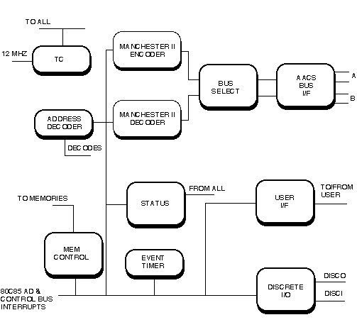
Fig. 1.2 IOU GA Block Diagram
There are a total of 76 signal pins which includes "Master reset, scan signals and parametric NAND tree signals." The ASIC uses an 84-pin ceramic flatpack with four power pins and four ground pins.
This section begins with a definition of terms and acronyms shown
below.
Use the following defintions for a quick reference.
AACSE		AACS corntrol Electronics
A/B		AACS Bus Select
BC IOU	Bus Controller Input Output Unit
C/C		CRAF/Cassini
EFC		Engineering Flight Computer
F.E.		Falling Edge
GA		Gate Array
ISB		Inter Subassembly Bus
I/F		Interface Face
RT IOU	Remote Terminal Input Output Unit
R.E.		Rising Edge
T/R		Transmit/Receive
F/W		Firmware
Note: In this document, unless otherwise specified, IOU => Both BC and RT IOU.
In this example, sections 3.1 to 3.7 of the specification describe the functional modules of the IOU gate array. Table 3-1 represents an IOU Memory Map, which is important information as an IOU user can use it to understand the allocation of the memory space. As a designer you want to describe the ASIC design explicitly, accurately, and in as much detail as possible. Use the specification of any standard VLSI component as a guide to write the details about the ASIC's functional description. Section 3.8 of the example specification lists the important IOU gate array worst-case timing specification from the user's viewpoint. These numbers reflect the results of extreme conditions such as worst-case condition at minimum voltage, high temperature, worst-case process and best-case condition at maximum voltage, low-temperature, and best-case process variations. The numbers in Table 3-2 do not reflect any guard bands from the point of view of a tester. The special section on AC characteristics also reflects the minimum and maximum AC parameters that a vendor has to guarantee in a manufactured device and those numbers reflect the vendor's tester guard bands.
TABLE 3-1 IOU MEMORY MAP
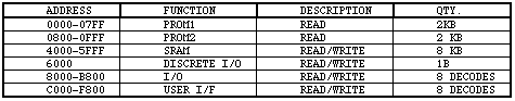
Table 3-2. IOU Gate Array Worst Case Timing Specifications
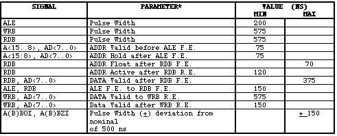
* These parameters are guarenteed by design but not necessarily tested. Refer to Sec. 5.5 "AC Characteristics" for the AC parameters tested by the Vendor.
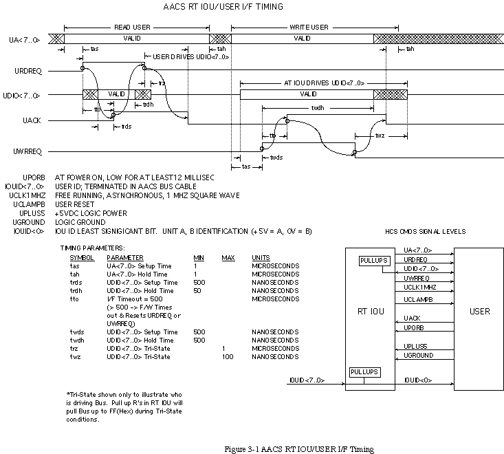
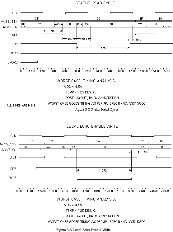
The following timing diagrams are provided for user reference to understand various cycles of this gate array.
Worst-Case Timing (continued)
Timing Diagrams: There are over a dozen timing diagrams in the IOU gate array specification describing various modes of operation including:
We have only shown three important timing diagrams for your reference here. On this page we show the AACS RT IOU/User Interface (I/F) Timing. On the following page we show the Status Read Cycle and Local Echo Enable Write diagrams. These are representative of good timing diagrams and show the significant functional activity relative to important clock and control signal changes.
For the I/O ring, an emerging standard is IEEE 1149.1 boundary scan approach. Please refer to the guide's Section Three: Chapter 3, on DFT details.
For the IOU gate array, full scan is used internally to aid in increasing overall fault coverage and its I/O signals have an IEEE1149.1-like boundary scan implementation. A NAND tree is implemented in the IOU gate array to facilitate Vil and Vih DC tests. A NAND tree is an approach for I/O characterization recommended by several ASIC vendors. Inclusion of a NAND tree in your ASIC design makes the generation of DC test vectors a simple task.
4.0 TESTABILITY CONSTRUCTS
4.1 Use of Scan: All of the latch elements used in the core area have scan capability. They are implemented using a multiplexer in front of every latch element to accept either system data or scan data. Scan elements are used to aid in increasing the overall fault coverage for IOU gate array. They are specially useful in dealing with long counter chains and to access and control some buried nodes. At the package level, there are several scan signals as described in Table 2-1 and listed below. They may appear to be in the same format as JTAG (IEEE-1149.1 standard for boundary scan), but this appearance is coincidental. There is no JTAG implementation on this device.
Scan Signals:
4.2 NAND Tree for DC Tests: To facilitate DC tests such as VIL and VIH, a NAND tree connecting all input pads and bidirectional pads (configured in input mode) is implemented on this gate array in accordance with the Vendor requirements. Refer to the vendor manual on "DC TESTING USING TREE CIRCUITS" for more details. "TESTDC", I/O pin #24 is assigned for NAND tree test.
Electrical Test Requirements: This table reflects all the applicable subgroups per MIL-STD-883 concerning pre-burn-in, post-burn-in, post 240 hour burn-in, etc.
5. Electrical Characteristics
5.1 Electrical Test Requirements
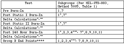
Table 5-1. Electrical Test Requirements
* PDA applies to these subgroups.
** Delta limits of Table VI herein shall apply.
*** Subgroup 4 (Cin and Cout measurements) shall be measured only for initial qualification and after process or design changes which may affect the value.
**** Group B.5 life test shall be performed using the dynamic burn-in configuration of fig. 3 herein. The table VI delta limits shall apply to the life test only.
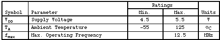
5.2 Absolute Maximum Ratings
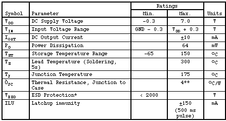
Table 5-2. Absolute Maximum Ratings
* ESD test method conforms to MIL-STD-883C, Method 3015, Electrostatic Discharge Sensitivity Test.
** This value is measured per Method-1012.
Note:
For example, if you are not using a triple-drive buffer in your design, you may want to leave it out of your list.
All exceptions and special conditions under which the device will be tested should be listed as footnotes.
5.4 DC Characteristics
5.4.1 DC Electrical Performance Characteristics
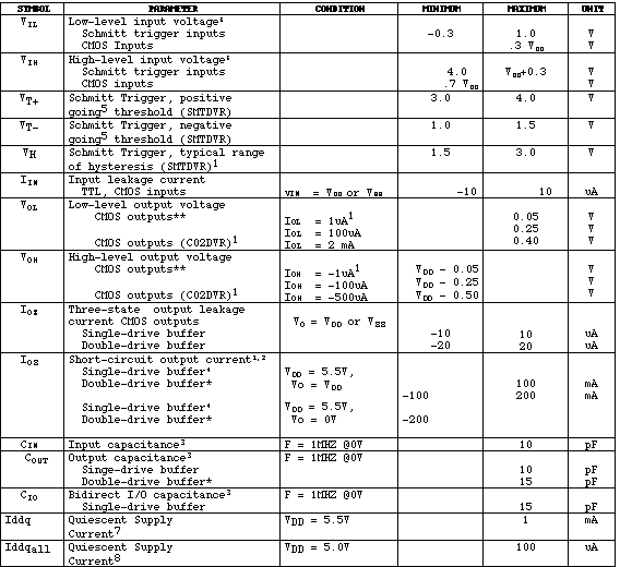 Table 5-4 DC Performance Characteristics
* Contact The Vendor prior to usage.
** If IOL and IOH exceed the max. limits for CMOS outputs, VOL and VOH will vary according to the sink or source current vs. VOL and VOH curve supplied by The Vendor.
Notes:
Pull-down and pull-up resistors: If you are using any internal pull- up and/or pull-down resistors, they should be listed. If IDDQ testing is one of your requirements, use any pull- ups or pull-downs in the core of an ASIC or in I/Os is highly discouraged as it makes the high-resolution current measurements required difficult or impossible.
5.4.2 IDDQ Testing.
Quiescent Current (IDDQ) testing shall be accomplished by using as close to 100% "Node Toggle Vectors" as possible which can be derived from the functional vecotrs or through a process determined by The Vendor and approved by JPL. Measurement stop points will be identified by JPL. IDDQ testing will be a GO/NO GO test. A single stop point shall be established for read-and-record measurements and delta calculations. The IDDQ limit is subject to change after device characterization. Refer to contract provisions for any exceptions to the qequirements stated here and IDDQ test program development, limits and screening of flight parts for IDDQ.
5.4.3 Pulldown Resisters.
Certain input pins are required to be held to a logic low state in flight.
There are no internal pull-down resistors used.
5.4.4 Pullup Resistors.
There are no internal pull-up resistors used.
5.5.1 AC Electrical Performance Characteristics
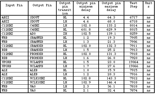
Table 5-5. AC Performance Characteristics
Note:
5.5.2 Timing Analysis.
Pre-layout and post-layout timing margins shall meet the contractor's requirements for timing analysis. Refer to "Additional Requirements" on page #6 for more details.
5.5.2.1 Pre-Layout Timing Margins.
Pre-layout timing margins shall be calculated by using standard extremem-value analysis. The extreme values for the cell library were supplied by The Vendor. Critical paths were identified before layout and margins were calculated via Valid or The Vendor software toolsets, or a combination thereof.
5.5.2.2 Post-Layout Timing Margins.
Post-layout analysis of the device shows positive margin on internal critical paths over all operating conditions. The analysis follows the same form as the pre-layout analysis, with the post-layout timing values annotated to the design file by the contractor. Timing parameters listed in Sec. 5.5 under AC characteristics are derived from post-layout data using actual wire lengths.
5.5.2.3 Tester Specification Limits.
Tester Specification limits in Table 5-5 have been adjusted for modified output levels and for differences in output loading in the Trillium tester environment. Modified output levels are required to account for impedance mismatches between device outputs and the Trillium tester environment. Refer to Figure 5-3 for switching test circuits and waveforms.
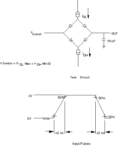
Figure 5-3. Switching test circuits and waveforms
Note: This capacitance is actually partially distributed through the fixturing so that the device is actually loaded by a transmission line.
5.4.1 Static Burn-In
The Static Burn-In conditions per MIL-STD-883 Method 1015 shall be as specified in JPL General Specification CS The Cassini ASIC Boilerplate Spec, Rev. C. The burn-in configuration shall be as shown in Table 5-6.
5.4.2 Dynamic Burn-In
The Dynamic Burn-In conditions shall be as specified in JPL General Specification CS the Cassini ASIC Boilerplate Spec, Rev. C. The burn-in configuration shall be as shown in Table 5-6.
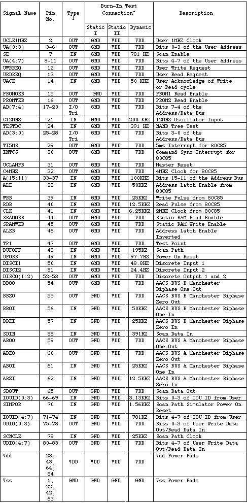
Table 5-6. Burn-in Connections
Notes:
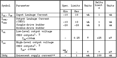
Table 5-7. Delta Limits
* Delta limits will be -10% of the min. values.
** Subject to change after device characterization.
Any exception to the standard vendor bonding diagram should be highlighted and approved by the ASIC vendor.
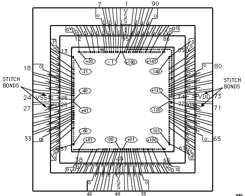
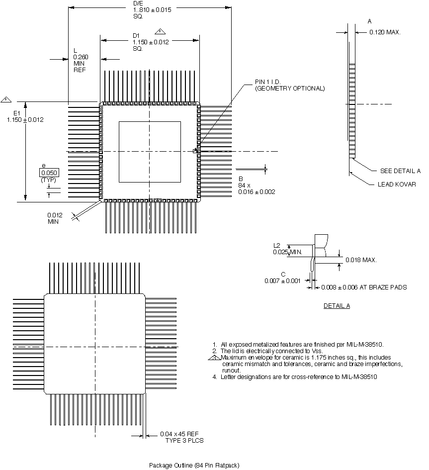
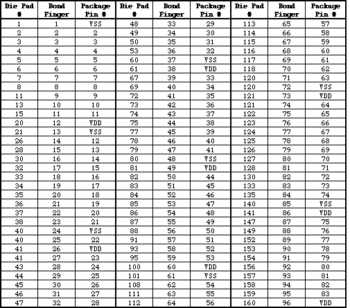
Table 6-1. Connections Table
(This is a die pad to bondfinger to package pin connection table for a 84-lead top-brazed flatpak)
Notes:
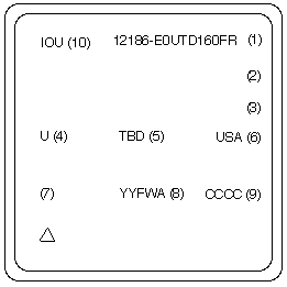
Fig. 6.4 Marking diagram
(1) The Vendor Part Number
(2) QPL Number (for flight unit only)
(3) Customer Part Number
(4) The Vendor Trademark
(5) Federal Supplier Manufacturing Number
(6) Country of Origin
(7) Pin 1 indicator and ESD identifier
(8) Date code - Year and Fiscal Week of Lid Seal. YY = Year, FW =
Fiscal Week, and A = Identifier for lots sealed within same week. ( A
- designates the second assembly lot of devices sealed within FWXX,
B designates the third assembly lot of devices sealed within FWXX
etc. The first assembly lot of devices sealed does not have a
designator.)
(9) Serialization (Traceability Capability to Die)
(10) Chip Name
-  Total Port signals			76

	Inputs				32
	Outputs				28
	Bidirects			16

-  Total VSS and VDD pins		8

-  Cell and block counts:

				Local	Global
		   Cells	131	1921
		   Blocks	231	13047

-  p and n-transistor counts:

			p: 13486	n:13399

-  Number of gates:			5624

-  Full internal scan

- Scan port signals provided to facilitate internal scan but there
   is no JTAG 1149.1 implementation.

-  NAND tree implemented for DC tests.

-  Functional patterns @1MHZ are used to achieve 98.1% Port fault
   coverage with ac delay measurements.

-  84 pin ceramic flatpack
The following are the applicable exceptions to The Cassini ASIC Boilerplate Spec.
Change "MIL-M-38510M" to "MIL-M-
38510".
Change "MIL-STD-883C" to "MIL-STD-
883".
Use Test method 1019.4 without TDE since it is specified and
approved.
Subparagraph a: The Vendor does not normally provide information regarding yield data. For QCI, The Vendor will provide summaries. Since group D is generic data, copies of the travellers are unnecessary.
Subparagraph b: Delete JPL approval rights since it has been agreed that JPL accepts The Vendor test tapes, but reserves the right to review them. The Vendor will provide a copy of the test flow chart, a detailed test module description, test program binary on tape, a copy of the test generation summary file, the test program execution summary file and will permit review of the test program source code and flow with JPL at the Vendor facility.
Section 3.10 PROBLEM NOTIFICATION
Under Subparagraph 3.10.a: The Vendor will inform JPL at interim
and post purn-in room temperature test failures.
Delete this paragraph since The Vendor processing flows are defined and controlled and no deviations are expected. JPL may review these flows at any time.
The Vendor uses a single golden unit with sufficient controls in place to obviate the need for three control units. Thus, in this paragraph all references to three control units are chaged to one.
The Vendor does supply a complete traveller, however, the lot specific traveller can be reviewed by JPL on-site.
Change "100 rads (Si) /s" to "100-300 rads (Si) /s".
The completed lot traveller can be reviewed by JPL on-site at The Vendor.
Now you may jump to: