Objective:
To provide ASIC managers with a structure to plan and
control the flow of an ASIC program.
As a manager, the success of your ASIC program rests upon sound
up-front planning and regular guidance.
Delivering a usable part calls for preventing multiple passes of
silicon, schedule slips, and budget overruns. To plan your program
right you need to understand the entire process of producing reliable ASICs, from initial
concept to part acceptance.
This section presents a framework for planning and controlling all
the essential processes and fostering the unique partnerships
between everyone involved in each step of the program. To ensure
the success of your project, you must properly establish this
framework with sound engineering and management judgment,
taking into account the specific requirements of your ASIC program.
Be aggressive in cultivating the sources of this "good
judgment." Make sure that you know your own organization's
ASIC resources. Don't hesitate to use the resources of your ASIC
vendors; the difference between a good ASIC vendor and a
commercial off-the-shelf (COTS) VLSI vendor is the depth and
experience of their customer support staff.
For managers interested in FPGAs, the last part of this chapter
outlines the guide's approach to these new devices.
The ASIC processes chart illustrates the steps and sequence essential
for a successful ASIC program. The ASIC manager must plan and
supervise each process, from setting requirements to delivery of
qualified flight ASIC parts. Figure 1.1.1 presents a flow of major
ASIC tasks.
The boxes in the top row represent the inputs to the processes.
The boxes in the center row of the flowchart represent the
processes.
Circled entities in the bottom row represent the outputs from that
process.
Note: Some processes generate outputs which are terminated.
Though shown in a rough chronological, single-threaded sequence,
the processes may interact in a more complex fashion. Some
processes may be completed once for multiple ASIC programs.
Others must be completed for every ASIC. Still others require
multiple iterations for a single ASIC program.
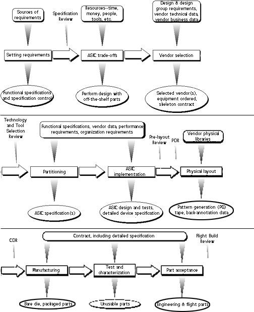
Figure 1.1.1 Tasks of an ASIC Program
A brief look at the central processes in Figure 1.1.1 follows:
Setting requirements focuses the work of an ASIC program.
When complete, the results of this process define the ASIC program
criteria and the ASIC's relationship to its system.
ASIC trade-offs ensure that use of ASIC technology will
provide a contribution to the ASIC's target system and to the overall
organization.
Vendor selection delivers the most important strategic
partner to an ASIC program.
Partitioning carves out the correct part of the system for
implementation as an ASIC.
ASIC implementation delivers a complete ASIC design and
associated design and test files.
Physical layout is ASIC design at the final level. The ultimate
results of this design work are fabrication masks used to build ASIC
parts.
Manufacturing produces ASIC dice assembled into
packages.
Test and characterization ensure that the manufactured parts
meet the goals of the ASIC design.
Part acceptance applies quality and reliability criteria to parts
delivered for flight use, screening out devices that show serious
potential problems.
The following are more detailed discussions of the processes in an
ASIC program.
Setting requirements provides the technical foundation that guides
all parties involved in producing a satisfactory ASIC. Often the
architecture or system design group provides the ASIC manager with
the requirements. Once set, these requirements generate the next
level of activity: assembling the necessary resources. Setting
requirements is the primary job of the ASIC manager. We
recommend accomplishing the following in conjunction with the
system-level design work:
- identify all sources of requirements
- propose a subsystem architecture
- derive functional specifications from a preliminary ASIC
partition of the subsystem architecture
- put specification control in place
- review specifications
For more on setting requirements, see Section Three: Chapter 2
REVIEW
At the end of setting requirements hold a specification review to focus on producing
clear and thorough ASIC specifications. Many times ambiguities in
the specification lead to second pass silicon. The ASIC may work well
as a stand-alone, but not in its target system. Since ASIC programs
have such long lead times relative to COTS VLSI parts, freeze the
specifications for ASICs and the interfacing systems early.
When a designer specifies an ASIC, managers must consider all the
trade-offs before approving the design. To determine if ASICs offer
the best solution, managers must weigh schedule, resources
(equipment, personnel, etc.) as well as performance, power, mass,
and board space budgets. Seeking information from groups with
previous ASIC experience can inject reality into a proposed ASIC
program. Check with an ASIC group within a NASA center, other
groups who have done ASICs, consultants, and ASIC vendors.
Perhaps ASICs may not be appropriate for the project. In this case,
the ASIC development flow terminates. If you decide to go with an
ASIC, then you must again return to a series of decisions regarding
implementation.
The major factors guiding system designers who choose ASICs
include: board space, performance, cost, and reliability. ASICs
provide many new ways to approach these issues.
Let's examine some of the trade-offs involved in implementing ASIC
methodologies and technologies.
Note: For those wondering about FPGAs, we are describing the
disciplines required to design with mask-programmable gate arrays
or standard cell ASICs. As FPGAs become qualified for space use
(radiation tolerance, sufficient proof of reliability, etc.), future
editions of this guide will discuss their use.
This guide considers two main approaches to ASIC design: gate array
and standard cell. However, over the past several years, ASIC
vendors have introduced a number of variations in architecture for
gate arrays and standard cells, such as "Sea of Gates,"
"Channeled arrays," and "Cell-Based Compilers or
Arrays."
In a gate array, the ASIC vendor prefabricates ASIC transistors in an
"array" and then fixes the array in position on a given
wafer (die). Interconnecting these transistors with metal wires in a
metallization process achieves logic functions. Typically, a designer
selects and interconnects logical elements (also known as cells) from
a gate array library; these have a predefined transistor design.
Sometimes a vendor will also supply a set of hard macros (super
macros) with a predefined circuit and hence predictable performance
parameters.
Gate arrays have resisted predictions of their demise over the last
ten years and have become the dominant form of ASIC technology in
terms of volume sold. A combination of ever-increasing gate
densities, low cost, first pass successes, and fast turn-around times
continues to make gate arrays the volume winner over standard
cells.
Each cell may differ in a standard cell ASIC. The vendor optimizes
the transistors for area and performance, predefines each logical
element, and makes "super-macros" available. As in the
gate array approach, design proceeds by selecting the proper library
cells and defining their interconnection.
The difference between gate array and standard cell ASICs lies in the
nature of the cell. Whereas the gate array cell consists of an array of
identical transistors, the standard cell consists of different size
transistors, optimized for the cell's function, allowing the standard
cell to have a smaller, faster cell for a given function than the gate
array. However, the desirable characteristics of the standard cell
require a completely new design at every layer of the chip. Gate
array chips differ only in the top metal-related layers.
For a qualitative comparison of different ASIC technologies and
processes, refer to Section Two: Chapters
2, 3, 4, and 5 and
Section Three: Chapter 2.
Vendor selection can determine the success of an ASIC program. An
unwise choice of technology, tools or vendor can prolong a schedule
and put severe strain on a budget. Section Two of this guide has
extensive discussion of vendor selection. We divide this activity into
technical and managerial selection criteria. For more information on
working with procurement on this and other ASIC activity, see Appendix Five: "Procurement
Support."
"How fast are their ASICs? How many usable gates can I get
for this offering? Do they support the Computer Aided Engineering
(CAE) software and platforms I have already invested in and am
familiar with? How much does it cost? How soon can I get my
parts? Will they be around for the next few years?" These are
some of the questions the ASIC team asks before the selection
process starts. Performance requirements, quality, reliability,
money, and time should govern your choice of vendors. While it may
be tempting to select a vendor with relatively fast published gate
delay data compared to the rest of industry, the astute manager will
take a more comprehensive look at vendor capabilities, including:
- vendor data on technology and tools
- vendor performance on important benchmarks for the ASIC
application
- inputs from previous users of the vendor
- inventory of available in-house CAE tools and input from CAE
tool vendors
Experience shows that it is wise to limit the number of ASIC vendors. It is not wise to switch vendors for
small incremental gains unless absolutely necessary because users
confront a steep learning curve for each vendor. Managing a vendor
proves a task in itself. Therefore, as an ASIC manager, it behooves
you to limit the number. You will invest time and effort to develop
productive working relationships with the vendors' applications, test,
and production personnel. These contacts become extremely handy
when problems arise--and they will.
REVIEW
Tools selection review takes place during vendor selection. Section
Two gives recommendations for forming an evaluation team to
conduct this review. The review assures all participants that the
correct mix of tools and technology is available to implement the
ASIC specification and satisfy all ASIC requirements.
The designers may partition the system functional specification into
one or more ASICs. They often do the partitioning in parallel with
"Vendor Selection" and "ASIC Trade-offs." To
aid these processes, you need to estimate the complexity of the
functional specification.
System architects and ASIC designers have a good idea of the general
partitioning from the time system level specifications are laid out,
though the specifications are generally incomplete at this point.
Accounting for system level interface and trade-offs when
partitioning avoids repartitioning in the middle of the design phase.
Test and performance requirements, global device specifications,
such as rad-hard specifications and testability specifications, must be
taken into account in functional partitioning.
For more on partitioning, see
Section Three: Chapter 2.
The element of design introduces the most
striking difference between using ASICs and off-the-shelf VLSI
components. For ASIC design, the guide places primary emphasis on
the optimum use of resources to satisfy specific performance and
reliability requirements. Consequently, design, along with its
verification and testability analysis, are the most important events of
an ASIC program. Verification includes simulation and test vector
generation, which play a key role.
The guide's methodologies focus on first-pass successful silicon. In
this guide, we define first pass silicon as: An ASIC device built from
the first preliminary design review (PDR) and
critical design review (CDR) design data base,
that works correctly in its system, both parametrically and
functionally, and requires no redesign. All processes in this flow
follow from this assumption.
For more on ASIC design, see Section
Three: Chapter 2. For details on modeling, see Appendix One: "Modeling and
Translation." For radiation issues, see Section Three: Chapter 4, along with the radiation appendix.
REVIEW
Two reviews occur during the ASIC design process: a schematic or
prelayout review and a PDR. The schematic review provides expert
confirmation that the design at this point, will satisfy the system and
other requirements. The PDR satisfies the vendor's experts that the
design is ready for successful layout.
"To determine if ASICs offer the best solution, managers
must weigh schedule and resources as well as power, mass, and
board space budgets."
When you arrive at layout the ASIC design verification should be
complete from your design group's perspective. After the PDR sign-
off and resolution of any outstanding device specific issues, the ASIC
vendor will perform, place and route, using their physical libraries
and the PDR-released data base. Vendors in most cases will
encourage the designer to participate in placing major blocks, critical
nets, and clock distribution networks.
Some vendors offer designers the choice of performing place and
route task themselves. Other vendors will not accept a client's
physical design data and require that they do the work themselves.
In the guide, we recommend the designer let the vendor perform the
physical design or place and route function. However, a standard cell
approach may be necessary for place and route.
After completing the layout, the designers review the back-
annotated resistance and capacitance values that arise from the
interconnects in the physical layout. These numbers reflect
reasonable estimates of the final design's worst case and best case
performance. This review consists of post-layout simulation and path
analysis to make sure no significant changes in function or
performance have occurred because of layout. The designers must
perform this analysis themselves as the vendor engineers lack
familiarity with the system application of the ASIC and are generally
unaware of the significance of minor variations in timing or other
performance.
In addition to the customer's post-layout analysis, make sure you
verify against the original system and device level specification. The
designer can supply the vendor with full functional tests and
comprehensive individual pin and pin-to-pin minimum/maximum
timing tests that absolutely ensure the successful operation of the
ASIC in its larger system. Most of the time the vendor's engineers
can modify the ASIC layout to meet these constraints, assuming the
design had adequate margins before layout. For more on physical
layout, see Section Three: Chapter
2.
REVIEW
A CDR takes place after completing the layout analysis. The CDR calls
for the customer's ASIC designer, the parts specialist, and the
technical contract manager to determine if the design and test data
base for the ASIC is complete and ready for the device to be built.
Note: Following the CDR, the vendor generates a pattern-generation
(PG) tape. After the PG the vendor expends significant resources.
Because of this incurred expense, typically the vendor requires the
equivalent to a "release to production," known as the
formal "chip sign-off." The sign-off notifies the customer
and designer that future changes will be expensive. At this time, the
device and test specification must be completed.
The manufacturing stage incurs significant expense. Vigilant
attention to the preceding steps will help this process remain cost
efficient, timely, and successful. The ASIC vendor will make masks
from the PG tape first and start the manufacturing process, which
consists of three phases: wafer fabrication, wafer probe, and
assembly process.
The vendor assumes responsibility for fabricating, probing and
sorting wafers, then assembles and packages good dice per
requirements. The vendor only involves ASIC managers or designers
in this process if there are problems discovered with wafer probe or
in the assembly process. The Qualified Manufacturers List (QML) and
Qualified Products List (QPL) programs cover a number of directives
concerning manufacturing processes.
The boiler plate and device-specific contracts, with the needs for
prototypes, engineering or flight parts, will determine the number of
wafer starts the manufacturer puts onto the manufacturing process
line. The vendor controls this process and notifies the customer's
ASIC program manager if there are deviations in schedule or if the
vendor encounters a fabrication problem. The vendor sorts good
wafers; from these good wafers, the customer accepts according to
the criterion specified in the contract. Good dice are then packaged
according to the contract. The vendor often has a standard minimal
test and screen for prototype parts.
The ASIC part the vendor supplies is required to meet the test and
characterization outlined in the contract. This means that the
customer's parts specialist must write the test and characterization
requirements in clear, unambiguous language. Section Four and QML and QPL
documents discuss test and characterization in great detail.
The vendor and the customer test and characterize packaged parts
according to detailed device specifications, the contract, and the
vendor's procedures. For Part screening tests discussions, please
refer to Section Four: "Part
Acceptance," QML part manufacture (MIL-I-38535), QPL
part manufacture (MIL-M-38510), and MIL-STD-883 documents. If
requested in the contract, the vendor assumes responsibility for
documenting unusable devices and their modes of failure in the End
Item Data Package deliverable.
Part acceptance procedures set requirements for manufacturers to
accept parts according to specified quality and reliability criteria.
Section Four, which covers part acceptance, discusses specific tests
required for either engineering parts or flight parts in detail. Usable
devices will be subject to the parts acceptance tests, quality
conformance inspection (QCI), or optional vector quiescent current
measurement (IDDQ testing) as well as any other
screening requirements called for in the contract for engineering or
flight parts.
REVIEW
After the customers have received delivery and analyzed the
engineering parts, a flight build review is
held. This review ensures that the vendor and customer have
satisfactorily resolved all issues that may negatively affect the
quality of flight devices. At a review, engineers examine issues such
as fixes, changes in customer requirements, and waiver status so that
the vendor can proceed to fabrication.
Contracting spans a number of the previously discussed ASIC tasks,
so we have left it until last. As an ASIC manager you need to
understand the strengths and limitations of ASIC contracting, both
formal contracting with the ASIC vendor and other outside
organizations and informal contracting with groups in your
organization.
Contracts determine the product that the manufacturer will deliver
and the required resources; they describe the electrical and
mechanical requirements, testing requirements, and radiation
requirements as well as the costs and schedule. Consequently,
contracting demands accuracy, particularly an accurate description of
the ASIC. Given the complexity of ASICs, this task may prove more
difficult than it sounds. We urge that you spend the time necessary
to ensure that the contracts clearly define the product you expect the
vendor to deliver.
The procurement group usually completes these contracts, but an
ASIC manager has to understand all these issues to support
procurement from the technical, cost, and schedule viewpoints.
There are two types of contracts: a general or boiler-plate contract
and a device-specific contract that contains a statement of work
(SOW) and device-specific references. The boiler-plate contract is
usually part of a procurement package and may apply completely or
partially to a particular vendor. The device-specific contract
discusses the design-dependent nature of an ASIC.
For example, a general contract defines all the generic requirements,
issues, etc., that apply to an ASIC vendor's gate array available in a
256 pin LCC. The Cassini program uses 11 of these gate arrays to
implement a variety of functions. Thus, there are 11 separate design-
specific contracts, each one defining its own SOW, its special needs,
and its detailed requirements.
Contracting within your organization contributes a great deal to ASIC
success. The most important contract within your organization will be
the technical device specification. This contract provides the basis of
agreement between the ASIC managers, the designers, and the
system group. Give it careful attention -- much more than that given
to a "theory of operations" or similar document you may
be used to working with for off-the-shelf-based system design.
Remember, the technical specification becomes the "data
book" for your ASIC. As such, it must have detailed functional
and parametric descriptions completed in a timely fashion so the
appropriate information is available for system design and outside
contracting.
For more on this subject and building a complete specific contract,
see Section Three: Chapter 1:
"Technical Specification."
FPGAs represent a new and promising technology for projects with
short duration and quick turn around that have moderate density
and performance requirements. These devices offer a cost-effective
way to bring ASIC technology to low volume systems that require a
consolidation of off-the-shelf "glue-logic" or functional
blocks of modest complexity. However, because of present
limitations, present FPGA technology cannot replace mask-
programmable gate arrays in every flight application.
FPGA devices consist of general purpose logic element arrays. In the
field, users configure these elements into various circuits by
programming logic cells and interconnections between them. Field
programming eliminates the interconnection mask fabrication step
required when using mask-programmable gate arrays. Thus, using
FPGAs drastically reduces design-cycle time.
At present, the industry offers four FPGA interconnection
technologies:
- Conventional fuses blown to leave the desired logic element
interconnects. These devices may not be reprogrammed.
- Anti-fuses (a low impedance connection) created to achieve
desired logic element interconnects. These devices may not be
reprogrammed.
- Latches that control a multiplexer or three-state buffer are
loaded with a controlling value to create the desired element logic
and interconnects. These devices require an additional memory
storage chip on-board to contain their interconnect configuration.
These devices may be reprogrammed.
- Electrically programmed and erasable structures, used to
establish element interconnects. These devices may be
reprogrammed.
The guide addresses the major steps needed to build a successful
ASIC program. However, the ASIC guide does not address the
intricacies or trade-offs involved in designing FPGAs. Gather this
information from such sources as:
- FPGA industry seminars
- text books on the subject
- college EE design courses
- Computer-Aided Design (CAD) tool vendor classes and seminars
Here we compare using FPGAs with using mask-programmable gate
arrays in a flight application.
Design
Four major differences exist between designing FPGAs and designing
mask programmable gate arrays: density, speed, granularity, and
design-cycle time. State-of-the-art FPGAs offer lower usable density
than mask-programmable gate arrays. FPGAs have approximately 10
times fewer equivalent gates. Also FPGAs run slower than mask-
programmable gate arrays.
As a rule, FPGAs run two to three times slower than equivalent
mask-programmable devices. Keep this in mind, as most FPGA
vendors quote very optimistic FPGA speeds in their specifications.
The level of granularity available to the designer differs for the two
types of devices. A mask-programmable device library has devices
(inverters) available with as few as two transistors. The smallest
FPGA library elements have at least twelve transistors. This can have
serious implications, especially when trying to resolve both too fast
and too slow timing delay problems.
When considering design cycle time, note that the mask-
programmable vendor has specific responsibilities in the ASIC design
loop after completing each design. The FPGA vendor, on the other
hand, normally has no direct responsibility after delivering the
unprogrammed devices. This lowers the cost and time required for
many aspects of an FPGA-based ASIC program.
Test
Testing FPGAs often requires programming the device before testing.
Testing FPGAs after programming presents difficulties not associated
with the same testing of mask-programmable devices. The vendor
can thoroughly test unprogrammed FPGAs as off-the-shelf devices.
However, testing FPGAs after programming identifies parametric and
logical problems not detectable before programming. Parametric
testing of programmed FPGAs requires specialized equipment that is
frequently not available to most design groups. Also designers must
often perform logical and functional testing of programmed FPGAs
in-situ. This prohibits using specialized stand-alone testers and
associated system-level test support equipment needed to exercise
all device functions through as many states as possible.
Present FPGAs have architecture and density limitations that usually
make design-for-test approaches (such as scan-design or IEEE
1149.1) too expensive. Therefore, test vector development can take
much longer for an FPGA design than for the equivalent design in a
mask-programmable gate array.
Here we address the similarities and differences between the ASIC
tasks for field-programmable gate arrays and mask-programmable
gate arrays.
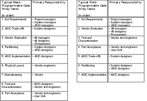
Table 1.1.1: Comparison of mask-programmable to
field-programmable gate array tasks and responsibilities.
Table 1.1.1 offers comparisons between FPGA program tasks and
mask-programmable gate array program tasks. This table shows that
an FPGA program requires two fewer tasks than a mask-
programmable gate array program--physical layout and
manufacturing. Tasks shared by both types of programs occur in
different sequences. Some other tasks appear in a different
sequence.
The following tasks are essentially the same for FPGA programs and
for mask-programmable gate array programs:
- Set requirements: What device-specific and system-specific
requirements must ASICs meet?
- ASIC trade-offs: What is the best mix of ASICs and off-the-shelf
parts?
Although required by both types of programs, the following tasks
have some minor differences:
- Vendor Evaluation: Unlike mask-programmable gate array
vendors, it is not necessary to evaluate a FPGA vendor for post-
layout back-annotation capability to a user's design system.
However, back annotation is done by FPGA software because this
software optimizes and reduces the hardware.
- Partitioning: Certain FPGA design features may drive a different
partitioning than for mask-programmable gate arrays.
- ASIC implementation: Again, FPGA design features may drive a
different design approach than used for mask-programmable gate
arrays.
The following tasks, while shared by both types of programs, have
some fundamental differences:
- Test and characterization: FPGAs undergo an off-the-shelf test
and characterization program by the vendor that does not require
user-generated test input. However, users are responsible for any
post-programming test and characterization.
- Part acceptance: Again, FPGAs undergo an off-the-shelf part
acceptance program, but any post-programming yield-loss and part
acceptance work is the responsibility of the user.
While necessary for a mask-programmable gate-array user program,
the following tasks are not part of an FPGA user program:
- Physical layout: For FPGAs this is done independent of the user,
typically long before the user selects a particular FPGA.
- Manufacturing: No part of FPGA manufacture requires any input
from the user or user's design.
Summary
- Rapidly evolving ASIC technology continues to drive changes in
electronic circuit design and system design, adding responsibilities to
all phases of an ASIC program, particularly design. The manager
must understand the impact of these changes and establish a broad
range of checkpoints to ensure that the program stays on track.
- The end (acceptable parts) depends on the beginning (planning).
The ASIC manager must plan and supervise each process from
concept to delivery.
- Setting requirements provides the technical foundation that
guides all parties involved in producing a satisfactory ASIC.
- The ASIC manager uses the detailed specification as a
"completion contract" with the ASIC designer. The SOW
and the detailed contract serve as powerful tools for clearly
delineating the ASIC responsibilities of other groups within the
manager's organization.
- Contracting determines the part that will be delivered.
Consequently, contracting demands accuracy, particularly when
describing the ASIC.
- There are two types of ASIC vendor contracts: the general or
boiler-plate contract, and the device-specific contract, which contains
an SOW and device-specific references. The boiler-plate contract is
usually part of a procurement package and may be completely or
partially applicable to a particular vendor.
- To determine if ASICs offer the best solution, weigh schedule,
resources (equipment, personnel, etc.) as well as performance, power,
mass, and board space budgets.
- Vendor selection can determine the success of an ASIC program.
Choose a vendor based on your requirements; don't base your choice
on other factors that may be impressive in the industry but do not
affect your requirements.
- Partitioning determines what part of a system will be
implemented by an ASIC or ASICs and what part will be
implemented by off-the-shelf devices.
- Design, along with its verification and testability analysis are the
most important events of an ASIC program.
- When you arrive at physical layout, the ASIC design validation
should be completed.
- The manufacturing stage incurs significant expense. Attention to
the preceding processes will help keep ASIC manufacturing efficient,
timely, and successful.
- The part that the vendor supplies should meet the test and
characterization that you outlined in the contract.
- Nothing can substitute for sound management and engineering
judgment. An ASIC program cannot hope to succeed without a
detailed consideration and careful weighing of all important tasks.
- FPGAs can provide very economical solutions to several
"glue-logic" ASIC applications. However, compared to
mask-programmable gate arrays, FPGAs must be used with full
knowledge of their environmental, performance, design, and test
limitations.
Now you may jump to: