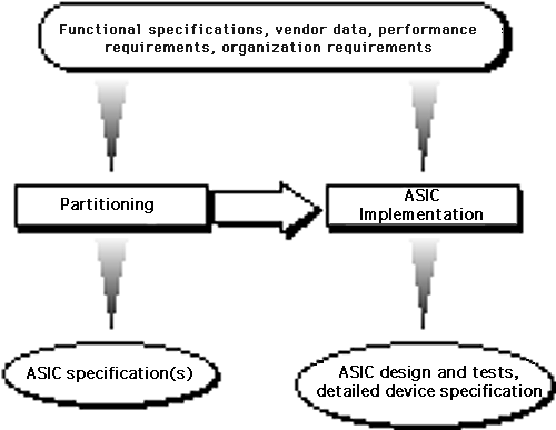
Figure 3.2.1 The ASIC Design Flow (For the complete flow, see Section One, Chapter 1)
This chapter presents sound engineering practices for the four major activities in the ASIC design process:
We will not discuss the basics of these four disciplines. Many first- rate avenues exist for learning these fundamentals:
We present ASIC design at a higher level, addressing design aspects unique to high reliability space applications. We emphasize information that designers may find difficult to locate elsewhere. For a perspective on how ASIC design fits into the overall ASIC flow, see Section One: Chapter 1: "Managing ASIC Development Tasks." Figure 3.2.1 shows the portion of the overall flow pertaining to this chapter.
Figure 3.2.1 The ASIC Design Flow (For the complete flow, see Section One, Chapter 1)
We begin by reviewing the design steps in the overall ASIC flow to orient the designer for the more detailed analyses to come.
When partitioning an ASIC, the designer must weigh off-the-shelf part capabilities against ASIC capabilities, taking the ASIC's much higher up-front costs into consideration.
The major ASIC-related factors that affect system partitioning with ASICs are:
The major system-related factors that affect system partitioning with ASICs are:
Make a rough requirements estimate to guide correct vendor and ASIC family selection. Later, during detailed system design, consider the ASIC family capabilities in deciding the final system partitioning.
Capabilities to weigh against costs include:
Standard Cells: Standard cells offer a designer the most function per die area and often more speed than a gate array implementation of the same design. At the same time, standard cell manufacture requires creating masks for every layer of an ASIC wafer's fabrication making sure each layer has corresponding unique fabrication.
Gate Arrays: Gate arrays require customizing only the layers of a wafer devoted to interconnect. This allows a vendor to build every gate array wafer identically to a point approximately 4/5ths of the way through fabrication. This minimum customization helps consistency and reliability. At the same time, gate arrays have fixed transistor sizes in their core regions, which limit transistor-level design choices for some functions. The fixed transistor sizes largely eliminates design with linear circuit elements.
Designers have little influence on the die area devoted to these partitions. At the same time, they must be aware of these partitions and how they limit the design. In some cases, a designer must designate approximate chip locations of certain functions to solve interconnect or power supply problems.
In some cases, a small design with a large number of I/Os will call for a bigger package, a bigger gate array and/or a larger die area to supply additional I/O.
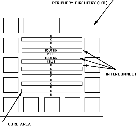
Figure 3.2.2 Generic Standard Cell Layout
Every ASIC vendor gives you some formula and data on which to base your calculations. Four components contribute to the overall power dissipation of an ASIC: Leakage current, crowbar current, current associated with the charging and discharging of capacitive loads, and dc current that comes from "on" transistors and the resistive current component.
Leakage current: Current that flows through an "off" transistor. This current is usually in pA and contributes to a very small percentage of the overall average power the chip consumes.
DC Current: Current that flows through "on" transistors, other than switching. Use of pull-up/pull down resistors, TTL loads (sourcing/sinking), floating gates or input pads, node contention on internal or external bus contribute to the DC current through a device. Minimize DC current as much as possible.
Crowbar Current: Current is caused during a transition when both the P-channel and N-channel transistors are partially "on." This current should be less than 10 percent of the total current. This is accomplished by minimizing the time the voltage swings through the on-voltage region for both N and P transistors.
Charging and Discharging Capacitor Current: This current is the largest component of the overall ASIC current and is due to charging and discharging of load capacitances. The power consumed by switching transistors is proportional to the operating frequency, the capacitive load, the square of the voltage swing, and the number of capacitive loads (internal gates or capacitive buffers). When a load capacitance CL is charged to a voltage V through a P- channel transistor, it stores a charge of CLV and energy of CLV2. This energy is dissipated when the capacitance discharges through an N-channel transistor. This charging and discharging takes place at a frequency "f." Therefore, the average current during switching and the power dissipated by a signal that switches each clock cycle are:
I = 1/2 fCLV
P = l/2 fCLV2
and for "n" nodes (signals) switching at the same time, it is "n" times the power component for one node.
Vendors usually provide power constants for each of the four major components discussed earlier. Leakage current is very small and not generally taken into account. DC current depends upon the number of pull up/pull down resistors used and the TTL sink requirements. This component is expressed, for example as mW/resistor used. Crow bar current is approximately 10 percent of the total current. For internal gates, ASIC vendors provide "microW/gate/MHz" number to be used. For input buffers a "microW/buffer/MHz" number is provided and for output drivers, it is expressed as "mW/Driver/MHz/pF."
Total power dissipation can be explained as:
P Total = Internal gate power + input buffer power +output buffer power + resistive power
P Total = (NINT x fINT x PINT) + (NIB x fIB x PIB) = (NOUT x fOUT x POUT) + (NRES x PRES x PRDY)
where:
NINT = Number of internal gates
PINT = Power per internal gate
fINT = Average operating frequency of the
individual gate
NIB = Number of input buffers
PIB = Power pre input buffer
fIB = Average operating frequency of the input
buffers
NOUT = Number of output buffers
fOUT = Average operating frequency of the output
drivers
NRES = Number of input pull-up or pull-down
resistors or output sink
PRES = Power per input resistor or TTL output sink
current
PRDY = Percent duty cycle that a pull-up or pull
down resistor is held in its high power state or output buffer is
sinking TTL current.
Example Calculation:
Number of internal gates:                           10000 gates
Number of gates switching each cycle (25%)          2500 gates
Number of I/O buffers used as outputs               80
Number of I/O buffers switching each cycle (25%)    20
Internal gate power (NINT)                          15 microW/gate/MHz
Output buffer power @ 50 pF load                    1.5 mW/drives/MHz
Number of input buffers                             50
Power per input buffer                              10 microW/buffer/MHz
Number of pull-up resistors                         16
Power per resistor                                  3 mW
(resistors are held in high power with a duty cycle of 25%)
Average operating frequency             =           10MHz
Internal gate power                     =           2500 x 10 x 15 microW
                                        =           375 mW
Input buffer power                      =           50 x 10 x 10 microW
                                        =           5mW
Output buffer power                     =           20 x 10 x 1.5 mW
                                        =           300 mW
Resistive power                         =           16 x 3 x .25 mW
                                        =           12 mW

P Total = (375 + 5 + 300 + 12) mW       =           692 mW
If the design was derived from another technology such as TTL, a one-to-one cell schematic correlation (TTL cell to MOS cell) probably will not be possible.
For example TTL cell clocking usually differs considerably from MOS cell clocking. In addition, TTL cell fan out may be much greater than the MOS cell. In general MOS cells are designed to drive small loads. To drive larger loads, an MOS design may need drivers not required on the equivalent TTL version. Similarly, the MOS drive for bus signals may differ significantly from the TTL drive shown on the schematic.
CMOS clocking often requires using 2-phase clock signals not generally required on TTL parts. Thus with standard cells the designer must implement clock generators and clock buffers to route the clock signals around the chip. With gate arrays the vendor should accomplish this implementation. In some cases, however, it may be the ASIC designer's responsibility.
Schematic capture also requires naming all wires, nodes, busses, and blocks. Naming expedites debugging the circuit under simulation. We also recommend using bus naming conventions when representing multiple signals on the schematic.
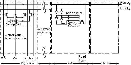
Figure 3.2.3 One bit of a 4-bit processor bus showing interconnects
Consider the pair of bus lines AK and BK. These signals must drive Cbus, the bus wiring capacitance. For a bus line whose length is 1000 lambda (a convenient unit, defined by Professor Carver Mead, representing the unit length of a chip's physical design), Cbus may not exceed 1 pF, which must be driven from the driver's P (pull up) or N (pull down). Therefore, allow sufficient time to charge the capacitance (Cbus) during a portion of the clock cycle. For this type of situation, carefully design the bus driver, bus line length, and clock periods.
Fan In: As the number of inputs to the gate increases, the speed performance of a basic MOS gate degrades. As a rule of thumb, implement logic gates requiring more than 5 inputs in two logic levels using basic boolean algebra transformation theorems.
Fan Out: The rise and fall times of a CMOS gate increase approximately linearly with increasing load capacitance. Therefore, place restrictions on the maximum number of loads driven from a single gate.
In general the gate's speed degradation, rather than the power dissipation, limits the allowable capacitive load at an output node. Therefore, in some designs require adding redundant logic to meet the speed requirements. The amount of redundancy introduced depends upon the application. We advise the designer to study each case carefully. Remember that each time you duplicate a gate, the fan-out of the previous gate increases. Therefore it may be necessary to add redundant gates all the way back to the source, and possibly all the way back to the input I/O pins.
The vendor supplies CMOS propagation delays sin their cell-library documentation.
To avoid reliability problems in some applications, high capacitive load drivers may require multiple Vdd and Vss I/O pins. This will depend upon the number of outputs switching simultaneously and their associated node capacitance.
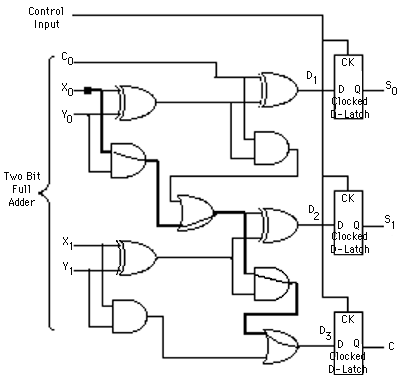
Figure 3.2.4 Data Skew Schematic
Note that all 3 D-Latches of Figure 3.2.4. have a common clock (Ck). This phenomenon mandates that all 3 data signals (D input) become true prior to activating the clock (Ck) signal. Since all 3 data signals (D input) originate from a different source and all 3 follow different logic paths, they will likely become true at differing times. For example, the path shown in bold from X0 to D3 has a longer delay than the path from X0 to D1 and may not present a valid logic level at D3 when Ck is active. This is referred to as "data skew." Data skew can cause false triggering and lead to false logic states. Solve the problem by making sure that the 3 data signals (D inputs D1, D2 and D3) become logically true prior to the Ck signal becoming true. This is most easily done by performing a pre- layout and post-layout timing analysis of the circuit under design.
Designers use the netlist to simulate a circuit. In addition to signal and device names, a netlist may contain device parameters that help in accurately simulating actual circuit behavior.
The reasons for simulation include:
Timing analysis simulation ensures that signals arrive at circuit elements and at the chip's pins at the correct times to produce the desired functions and performance. Two types of timing analysis are static timing and dithering.
Static timing analysis: This analysis consists of adding all signal delays of a particular path through a circuit to see if a particular signal change produces different results if that signal path has zero delay or non-zero delay. Good timing analysis tools greatly speed up this task, which will be repeated for many paths in a design. Certain "critical" paths that have multiple logic levels that are especially vulnerable to problems in this area.
Once identified, static timing analysis reanalyzes these critical paths a number of times using increasingly accurate timing information. These types of information include: high and low temperature delays, post-radiation delays, pre-layout interconnect, and post-layout interconnect delays.
Dithering: This is another approach to timing analysis on clocks and other critical signals. This analysis incrementally skews or "dithers" signal edges to identify which circuit elements prove particularly sensitive to small changes in signal timing. Where necessary, the dither approach improves the performance of these signals. Dithering commonly applies to setup and hold circuits to characterize their performance. See Figure 3.2.5 for a picture of setup and hold timing.
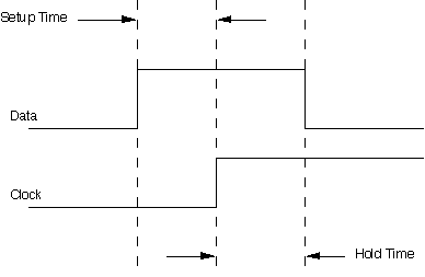
Figure 3.2.5 Setup and Hold Timing for any circuit using a clock to
acquire data
High-reliability chip design uses simulations extensively to demonstrate the chip test quality.
ASIC vendors require numerous design simulations to demonstrate ASIC "producibility" of an ASIC. These simulations often produce extensive negotiation between the vendor and designer to determine who will perform them and which ones will be required.
"Design Verification," which follows, discusses simulation in greater detail.
We briefly describe the advantages below:
Architecture: Hardware prototype architecture rarely reflects the final ASIC architecture. Therefore, using a hardware prototype may require several versions prior to the ASIC's final emulation. Designing and fabricating these hardware prototypes can be very costly and time consuming. Designers can often generate these prototype versions with simulators by rearranging hardware description language (HDL) code.
Design Exploration: The simulator enables the designer to explore design options, by making fairly minor simulator code changes, before committing to hardware. Exploring these options using hardware can prove difficult, costly and time consuming.
Non-destructive Analysis: Simulators operate on a logic-based mathematical model of an ASIC circuit. Simulations can be rerun many times prior to fabrication of the physical circuit.
Compare this to hardware debug of a prototype ASIC chip, which can be hazardous, especially if interior electrical probing is attempted. Though possible with the proper tools such as logic analyzers, pattern generators, probe equipment, etc., hardware trouble-shooting is cumbersome, often inaccurate or impossible, and can easily destroy the prototype chip.
ASIC Cell Emulation: Hardware prototypes cannot accurately emulate bare cells in an ASIC cell library. Vendors fabricate ASICs with micron or sub-micro devices and interconnects. This yields component values (such as stray capacitance) that hardware prototype cannot accurately model. Inaccuracy causes hardware prototype performance degradation. To overcome this problem use good simulators, which can provide accurate hardware modeling.
Logic Fault Emulation: Using simulation, designers can quickly simulate logic faults in the circuit and view the performance of the "faulty" device via software. This is an invaluable tool in creating the "high-fidelity" tests needed to ensure the delivery of defect-free devices. Reliability tests are difficult or impossible to develop without these types of computer simulations.
Multiple Device State Capture: Simulation methodology also provides the ability to capture many internal device states (past and present) at the same time. To do this with a hardware prototype requires multiple probes, logic analyzers, and special purpose hardware, which quickly become cumbersome with large systems.
Parameter Modeling: Simulation methodology also enables the designer to model worst-case parameters (such as temperature and process parameters) by changing a single software parameter and to quickly monitor the results. Again, this task proves difficult to do with hardware prototypes.
Time to Market: In the present electronic development era, products must be brought to market expeditiously. The loss of even a few weeks in development, can bring disastrous consequences to ASIC based products. Using simulation tools can accelerate the ASIC development and dramatically improve product time to market.
ASIC design poses an entirely different problem. A hardware breadboard cannot accurately resemble the final product, primarily because the parasitic components of a hardware breadboard differ completely from ASIC parasitic components. For this reason, ASIC breadboards often yield inaccurate characterizations. Extensively probing an ASIC to determine unacceptable design proves virtually impossible due to the ASIC's small size. Because of these problems, electronic circuit simulation has become the dominate design and verification tool for ASIC devices.
An electronic simulator represents the circuit components with mathematical models. The designer provides the simulator with a circuit component description along with circuit electronic input stimuli and chooses which analyses to perform. The simulator then performs numerical analysis procedures on the models, using the input stimuli, and generates predicted outputs. With this technique, the simulator can predict circuit performance results that are virtually impossible to obtain with laboratory measurements.
Whether that breadboard uses SSI and MSI logic devices or field programmable gate arrays, breadboard circuit timing measurements, can only approximate the final device's timing. Only through thorough circuit signal timing analysis, using post-layout timing information, can a designer be confident the design will deliver the desired function and performance.
Only the verified design and then the resulting part passing tests can demonstrate successful ASIC design, whether in its target system or in some other test configuration. Therefore, ASIC designers must be concerned with testing. Design-for-test techniques can often greatly simplify and accelerate testing and making tests for ASICs. Designers must often generate their own tests, driving their own self-interest to make a design as testable as other considerations will allow.
At certain stages in the design process, testing begins, starting with test generation. This task should be simultaneous with the initial architectural chip design. To wait until chip fabrication to worry about test generation only ensures a painful, lengthy test generation process that may not assure the design's quality.
Figure 3.2.6 (a), which shows a combinational circuit with n-inputs, best illustrates the problem of testing ASIC circuits.
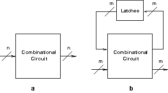
Figure 3.2.6 Combinational (a) and Sequential (b) Test Block
Diagrams
To test the circuit in Figure 3.2.6 (a) exhaustively, apply a sequence of 2n inputs (often referred to as test vectors) while observing the circuit outputs. It is not uncommon for n to be large in an ASIC design. For example if n = 25, then 225 = 33 million test vectors would be required to exhaustively test this circuit, making test time for such a circuit unmanageable. Unfortunately adding sequential logic accentuates the problem. Figure 3.2.6 (b), demonstrates this showing the previous combinational circuit appended with memory (m-storage latches for this example). Adding memory, the memory elements' inputs and previous state determine the circuit's state. To test this circuit exhaustively, apply a sequence of 2n+m test vectors to the circuit. For an ASIC circuit with n = 25 it would not be uncommon for m = 50. Thus 225+50 = 275 test vectors would be required. 275 is approximately equal to 3.8 x 10²². Thus to test this circuit at a 1 microsecond rate per test vector, would take over a billion years (109)! Clearly test time dictates utilizing methods for minimizing test vectors.
ASIC test generation depends highly upon the device under test. This device under test may contain the following circuit types:
The test generation will vary according to the circuit types requiring testing.
A "stuck-at" fault refers to a fault in a circuit logic model where a logic element's input or output is "stuck-at" a logical 1 or 0, switch between the two logical states, as in the "good" circuit logic model. This corresponds to many possible defects in a chip that all cause a short between a signal and power or ground.
We can presently analyze the "good" circuit model versus the "stuck-at" circuit model for circuits of great complexity. Unfortunately, generating tests to accomplish this analysis proves difficult unless a circuit has been designed with some type of sequential circuit partitioning. See Figure 3.2.6 and its accompanying discussion.
When a designer follows proper design partitioning techniques, many vendor tools provide automatic test vector generation or ATPG for SAFs. This automatic technique produces signals at input pins that both drive circuit nodes to 1's and 0's and propagate the results to output pins. In the language of stuck-at fault testing, a test set that produces the desired values at a node is said to have "controllability" of that node and a test set that propagates the test result to an output pin is said to provide "observability" to that node. ATPG tools, in conjunction with proper design techniques, can create test sets that give controllability and observability to most of a circuit.
A measure called "fault coverage" determines a fault test set quality. This measure comes from the ratio of the number of circuit nodes controlled and observed by a test set to the total number of nodes in a circuit. Scan design, a commonly available design technique supports ATPG scan design.
Scan design builds all sequential circuit elements (latches, flip-flops, etc.) into one or more large serial shift registers. These shift registers clock the tests generated for combinational circuit elements into place and reads the results, while they simultaneously test the sequential elements.
To create a thorough ASIC functional test, first test all functional blocks ASIC, including all significant data values. While an exhaustive functional test (testing all states, including those caused by differing data values) is not possible, a comprehensive functional test will exercise all desired functional states and all data values that correspond to limits (dynamic ranges) and structural activity (look-ahead, carry, etc.).
IDDQ test vectors provide a high "toggle coverage." Toggling refers to the test's ability to cause circuit element inputs to transition from a logical 1 to a logical 0 and visa versa. Toggle coverage expresses the ratio of the number of inputs toggled to the total number of inputs in a circuit for a particular test set. Recent published data from a number of companies show that defect levels may drop as much as two orders of magnitude when combining IDDQ testing with conventional stuck-at fault techniques.
Packaging must largely depend on the available packages a vendor can supply for a particular standard cell or gate array size. The guide recommends using only vendor standard packages, as qualifying a package proves a long and expensive process that can add significant overhead to an ASIC program.
The fundamental elements of packaging are:
Now you may jump to: