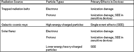
Table 3.4.1 Summary of Space Radiation Evironments and their Effects on CMOS Devices
Rad-hard ASICs must be designed for optimum performance and reliability in both non radiation and radiation environments encountered during the mission. This chapter discusses radiation hardening methods for ASICs using CMOS technology that must operate in the natural space radiation environment.
Table 3.4.1 Summary of Space Radiation Evironments and their
Effects on CMOS Devices
Although each particle interaction produces a number of electron- hole pairs, the total charge from a single particle interaction is generally too low to cause significant damage in current device technologies. Consequently, total dose degradation usually results from the aggregate interactions of a large number of protons or electrons within the regions of CMOS devices.
In general, devices become more sensitive to SEEs as they are reduced in size because they require less switching energy. Highly- scaled devices may be susceptible to SEEs from protons as well as heavy ions. This increases the SEE rate significantly because of the proton belts. Thus, SEEs are transient phenomena, triggered by a single high-energy particle interacting with p-n junctions within a semiconductor.
In addition to SEEs and TID effects, ASIC vendors sometimes design for radiation effects not considered in this chapter, which come from man-made nuclear events.
The manufacturer's specific techniques for fabricating each layer strongly affect ASIC hardness. Design techniques have some effect on hardness, but only limited improvements can be implemented at the circuit design level. Circuit design cannot overcome global failure of internal transistors due to field- oxide inversion, or compensate for large collection volumes for SEU charge generation. However, designers must know hardening techniques; using the wrong design methods may inadvertently lower radiation hardness to levels far below the level that a specific process can achieve. The following three approaches improve the radiation hardness of ASIC designs:
Radiation hardening involves a number of trade-offs. It requires either expensive base-wafers, more power than equivalent non-hard circuits, or more chip area than non-hard circuits. The designer may achieve radiation hardening using a combination of all three approaches listed above. To properly make potentially expensive trade-offs, designers must consider the radiation environments the ASIC will confront during operation, the system requirements for allowable charged-particle upset rates, and the allowable parametric shifts over the life of the device.
To get the maximum radiation tolerance for the minimum overall impact on other aspects of their device, designers will benefit from working closely with their ASIC vendors. Vendors with a proven radiation-hardened process, radiation-hardened cells, and radiation-aware design tools can provide ample information for the user to study the trade-offs involved in rad-hard design. Such trade-offs include: radiation tolerance, cost, ship area, electrical performance, and power dissipation.
Along with trade-offs, the user and the designer must anticipate radiation requirements near the beginning of an ASIC project. Doing so will help guide ASIC vendor selection and determine whether a commercial process can be used instead of a process specifically designed for radiation hardening.
Also, when contracting for ASIC part acceptance, clearly negotiate and specify radiation requirements to ensure proper testing and adequate hardness of devices. Finally, to use hardening economically, allow for radiation requirement trade-offs during the design phase, both at the system and individual ASIC level.
Appendix Three contains more information on the physics of radiation effects on microelectronics.
Ionization produces electron-hole pairs within insulators and semiconductors. The effect of the ionization on MOS devices depends upon the way that this charge is transported and trapped at the silicon-silicon dioxide interface. The net effect of ionizing radiation on MOS device oxides depends upon the oxide thickness, the field applied to the oxide during and after exposure, as well as trapping and recombination within the oxide. The manufacturing processing techniques strongly affect the latter factor.
Bias conditions have a large effect on total dose degradation. A positive gate-to-silicon oxide field will cause holes to be transported to the silicon-silicon dioxide interface, where some fraction of them will be trapped. A negative field will cause the holes to be transported to the gate, where they recombine with electrons and do not create hole traps. For n-channel devices, this worst-case condition for hole transport and trapping requires positive voltage at the gate relative to the source (device biased on). For p-channel devices the worst-case condition is negative gate-to-source voltage, with the device biased off.
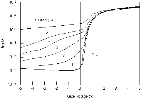
The trapped holes at the silicon-silicon dioxide interface change the threshold voltage. For n-channel devices the threshold shift is negative, causing a transistor to gradually shift toward depletion mode as the total dose increases. P-channel devices shift in the opposite direction. Figure 3.4.1 shows these effects for a typical commercial process: hardened devices will exhibit much lower threshold shifts primarily because of recombination in the oxide. Present commercial CMOS technologies will usually fail at levels between 10 and 50 krad(Si).
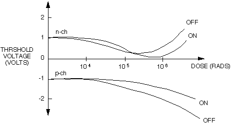
Figure 3.4.1 Voltage shifts due to irradiation
In practice, total dose effects in MOS devices are much more complicated than the elementary description of hole trapping described above. In hardening a process, the vendor needs to take three additional factors into account:
Substantial variations in hardness may occur between different lots, particularly for commercial processes, which usually do not include radiation hardness as part of their process control. The radiation response will be affected by oxide thickness as well as by changes in the specific way that either gate or field oxides are grown during the fabrication process. The hardness of commercial processes may vary substantially between different processing lots.
During vendor evaluation, the evaluating team should examine radiation data carefully, paying particularly close attention to the dose rate, bias conditions, and time periods used for testing. Data on complex circuits is often difficult to interpret. Often subthreshold I-V curves for test transistors are used to evaluate total dose hardness. When using this approach, the vendor exposes the device to radiation (usually Cobalt-60 gamma rays), under bias. I-V curves are measured after predetermined total dose levels. To characterize the subthreshold region, I-V curves should be taken over many decades of drain current. The subthreshold region can be used to separate the effects of trapped charge and interface traps, providing a good reference point for evaluation of total dose hardness of different processes or different processing runs. When evaluating specific processes, the evaluators must consider total dose effects on both gate and field oxides.
One way to accommodate threshold voltage shifts after irradiation is to change the relative area of the p- and n-channel devices. Normally a CMOS inverter will be scaled with a 2:1 ratio between p- and n-channel devices. This scaling compensates for the difference in hole and electron mobility in silicon and thereby provides comparable drive under normal conditions. Changing this ratio can increase the tolerance of a circuit to post-radiation changes in threshold voltage. Figure 3.4.5 illustrates this technique.
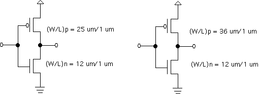
Figure 3.4.5 CMOS inverters
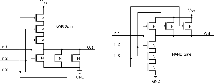
Figure 3.4.6 Comparison of NOR and NAND gate transistor
implementations
With radiation, the n-MOS transistor may become leaky. Also, both transistors may lose drive capability due to mobility degradation. For the NOR gate, the increased channel-leakage currents through the parallel connected n-MOS transistors will increase static power dissipation when all inputs are LOW. In addition, the reduced current drive of the series-connected p-MOS transistors will seriously degrade the charging response of the output node to a falling input signal. Increased leakage currents flowing through the n-MOS transistors further degrade the charging response. Decreased charging response stretches out the output node rise time. Thus the NOR gate may not respond fast enough to a falling input signal and a functional error may result. These failure mechanisms make NOR gates the circuit type least tolerant to radiation. The NAND gate, on the other hand, does not have these problems because the n-MOS and p-MOS transistors are reversed from that of the NOR gate. In Co- 60 tests, NAND gates retain a higher fraction of the original noise margin with radiation than the NOR gate. Thus, designers prefer the NAND logic gate for hardened circuit designs. If NOR gates must be used in circuits designed for rad-hard environments, then minimize the number of inputs (fan-in).
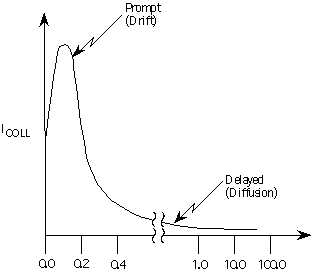
Figure 3.4.7 SEU response illustrating collected current pulse
shape
The effect of these random charges on the circuit depends on a number of factors, including the minimum charge required to switch a digital circuit. If the energy deposited by the ion exceeds the minimum charge (critical charge), then the passage of the ion will upset or otherwise affect the circuit.
High-energy particles can induce a number of effects. Not all of these effects are possible in all devices either because the critical charge for the effect is too high, or because the specific design (or processing) of the circuit precludes the occurrence (e.g., latchup in silicon-on-insulator technology). These effects can be subdivided into two basic categories:
These categories are discussed in more detail below.
The galactic cosmic ray environment consists of a distribution of different particle types with different ion species and energies. The number of particles falls off rapidly with increasing LET, as shown in Figure 3.4.8. There are very few particles with LET > 26, the so-called iron threshold. Thus, if the threshold LET exceeds the effective LET of iron at more extreme angles (near 80 MeV-cm2/mg), the error rate will be low.
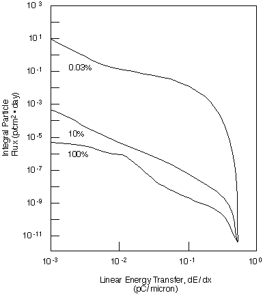
Figure 3.4.8 Galactic cosmic ray environment at geosynchronous
orbit
The error rate is often expressed in errors per bit day. The error rate of hardened devices can be on the order of 10-8 errors/bit-day or lower. The error rate of unhardened devices is generally several orders of magnitude greater.
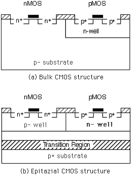
Figure 3.4.9 Cross-sections of bulk and epitaxial CMOS processes
The only difference between the two processes shown in Figure 3.4.9 is that one is fabricated on a highly doped p+ substrate. The highly doped substrate reduces substrate resistance, making latchup less likely compared to standard bulk processes. The low-resistivity substrate also reduces the amount of charge that can be collected from the n+ drain, which improves single-event upset hardness compared to bulk processes.
Figure 3.4.10 (a) and (b) shows two CMOS structures that eliminate the junction-isolated well structure, thus eliminating the possibility of latchup. These structures also reduce the charge collection region, further improving single-event upset hardness. The first process is silicon-on-sapphire (SOS), which results in two separate p- and n-doped islands on an insulating sapphire substrate. The second process is silicon-on-insulator (SOI), which uses special processing to grow an isolated silicon dioxide insulating layer on a bulk silicon substrate. Both structures substantially improve single-event upset hardness, and eliminate latchup. However, neither process is used in significant volume, and they are both highly specialized, costly processes. Thus, ASIC processes that use them should only be selected when the radiation requirements are sufficiently high to justify their use.
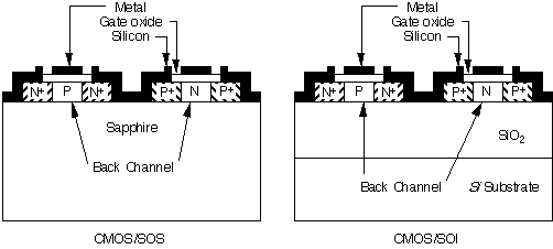
Figure 3.4.10 Cross-sections of CMOS/SOS and silicon on insulator
(SOI) processes
Originally, only heavy ions caused SEU effects. However, as individual transistors were scaled to smaller dimensions to increase the size and complexity of VLSI circuits, their susceptibility to SEU effects increased. If the sensitivity increases sufficiently, devices can be upset with protons (through nuclear reactions) as well as with heavy particles. This increases the upset rate by many orders of magnitude because of the large number of protons in solar flares and in trapped radiation belts.
There are two ways to harden a circuit against SEUs: (1) Reduce the charge that the node can collect by using processes such as SOI, SOS, or bulk epitaxial substrates, and (2) Increase the charge necessary to produce an upset by increasing the device area or by introducing special circuit techniques (such as decoupling resistors).
Multiple-Bit Upset: For some technologies, such as DRAMs or certain SRAMs, the ionization track from a single particle may cause several storage elements in a circuit to upset. This is called "multiple-bit upset." This phenomenon is more difficult to deal with than SEU because the multiple errors may interfere with system-level approaches such as error-detection-and-correction (EDAC) that are often used to overcome SEU effects.
Single-Event Transients: Besides the effect on storage cells, single-event interactions can produce transient output pulses in combinational logic circuits that do not contain internal storage elements. These transients are usually of short duration (about 1 ns), but may indirectly produce changes in the state of other circuits if they occur at critical time periods, such as during clock or data transitions.
Designers have successfully implemented several methods to increase the charge the node must collect (QCRIT) to cause upset. These methods have included the adding capacitors, resistors, transistors or combinations of these devices to the circuit. As a penalty, these additional components generally cause increased circuit area and decreased circuit speed, and these drawbacks must be traded off against the increased SEU hardness. Table 3.4.1 illustrates resistor, capacitor, and transistor hardening techniques for an SRAM cell.
Decoupling resistors have been used to harden older processes to SEU. This approach is less effective with newer technologies because of the penalty on area and switching speed.
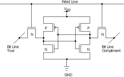
Figure 3.4.11 Six transisitor CMOS static random access memory
(SRAM) cell
This circuit's SEU-sensitive regions are the strongly reverse-biased P+ region when the data node is LOW, and the strongly reverse- biased N+ region when the data node is HIGH. Adding resistors as shown in Figure 3.4.12, introduces additional time constants that filter out the effect of the very fast SEU-induced transients. The polysilicon decoupling resistors (R) slow down the bistable flip-flop's regenerative feedback response. Although resistive hardening can be successful, it is somewhat difficult to implement in practice because of the high temperature coefficient of the polysilicon resistors, as well as difficulty in controlling the variation of the resistors within a specific process.
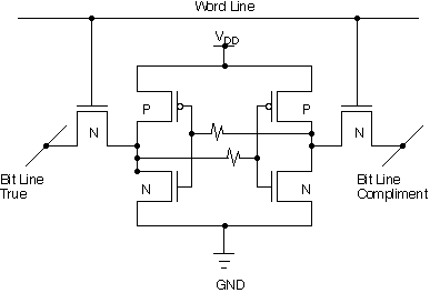
Figure 3.4.12 Resistive hardened CMOS SRAM cell
Be careful. Many CMOS design approaches have circuitry sections that use resistors, rather than p-channel transistors, as loads for their n-channel devices (four-transistor memory cells). This practice produces a faster, denser and lower power cell compared to a six- transistor memory cell, but the 4-T circuits are much more sensitive to radiation because of the high-resistance path of the resistive loads. Therefore, avoid them in rad-hard designs. Similarly, experience shows that depletion-mode load devices and dynamically held node circuitry should be eliminated from the rad-hard library of potential design elements.
System designers will want to know at what rate your ASIC will upset in a given radiation environment. These upset-rate calculations are complex. Work closely with your vendor or, perhaps, make the device upset rate calculation a deliverable from the vendor after performing place and route.
Predicting upset rates for ASIC designs is difficult because the SEU sensitivity depends somewhat on the way the design is implemented. Circuit modeling can also be used to predict the effect of different designs on SEU hardness. Highly accurate upset rate predictions require testing each design in a particle accelerator, such as the Brookhaven Van de Graaff. Although expensive, such testing provides basic characterization information about the SEU response that can be used to calculate the upset rate in the anticipated space environments.
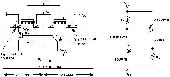
Figure 3.4.13 Source of latchup in CMOS
Once latchup occurs, the four-layer structure will be switched into a conducting mode, and will remain in that mode until power is removed. During latchup currents can be very high. In most circuits, currents of several hundred milliamps or more will flow in the localized region where latchup is triggered, rapidly heating that section to extremely high temperatures. These high temperatures not only introduce the possibility of localized damage to the silicon and metallization, but the excessive heating may also cause the latchup to spread to other regions.
Because of the potential for catastrophic damage, latchup poses a very serious problem for space systems. The most conservative approach tests samples of each device type, and disallows use of any device that exhibits latchup. A number of methods have also been proposed to overcome latchup at the system or subsystem level by sensing excess current, which is a signature of latchup, and temporarily removing power. However, the power must be removed within a few milliseconds after latchup occurs to avoid possible catastrophic damage to the device metallization or bonding leads.
Heavy-ion latchup testing is done using a particle accelerator, by placing the device in a vacuum chamber connected to the accelerator. Latchup is detected by monitoring both the power supply current and functional operation while the device is being irradiated with the accelerator. The range of ions used for latchup testing should be 40 microns or more. Sources with more limited range (such as californium fission sources) should not be used.
These techniques will generally raise the minimum LET at which latchup will occur, but are not always successful in reducing latchup probability to acceptable levels. It is very difficult to analyze latchup conditions in circuits. For example, earlier literature claimed that latchup could not occur in processes that used epitaxial substrates. Later test results showed that this was not necessarily true.
The only certain way to eliminate latchup is to use an SOS or SOI CMOS process that eliminates one of the parasitic transistors, thereby removing the possibility of latchup.
Problems with SELs fall into two categories: immediate or latent damage, and reduced system functionality.
Power cycling and reinitializing may be acceptable with a very low latchup probability, but will generally be unacceptable if latchup occurs frequently. There may also be critical phases of a mission during which latchup and power cycling cannot be accommodated, because there is insufficient time to recover within the operational window.
Although design techniques can influence radiation hardness somewhat, the largest single factor in determining radiation hardness is the method of implementing the process. Special, radiation-hardened processes are available that can function at much higher levels than commercial ASIC processes, although they are more costly. A key step for designers is to establish the required level of hardness and then match that hardness to the process. Designers must pay particular attention to this match taking into account the environmental level and other key factors, such as latchup or EDAC compatibility. Once a specific process is selected, it is very difficult to increase hardness later. In fact, requiring increased hardness may mean starting over.
H. E. Boesch, Jr., and T. L. Taylor, "Total dose induced hole trapping and interface state generation in field oxides," IEEE Trans. Nucl. Sci., Vol. NS-31, no. 6, Dec. 1983, pp. 1273-1278.
J. S. Browning, R. Koga, and W. A. Kolasinski, "Single event upset rate estimates for a 16-k CMOS SRAM," IEEE Trans. Nuclear Sci., Vol. NS-32, no. 6, Dec. 1985, pp. 4133-4139.
S. E. Diehl-Nagle, "A new class of single-event soft errors," IEEE Trans. Nucl. Sci., Vol. NS-31, no. 6, Dec. 1984, pp. 1145- 1148.
S.E. Diehl, A. Ochoa, Jr., P.V. Dressendorfer, R. Koga, and W. A. Kolasinski, "Error analysis and prevention of cosmic ion- induced soft errors in static CMOS RAM's," IEEE Trans. Nuclear Sci., Vol. NS-29, no. 6, Dec. 1982 , pp. 2032-2039.
T.P. Haraszti, "CMOS/SOS memory circuits for radiation environments," IEEE J. Solid-State Circuits, Vol. SC-13, no. 5, Oct. 1978.
A. H. Johnston, "Super recovery of total dose damage in MOS devices," IEEE Trans. Nuclear Sci., Vol. NS-31, no. 6, pp. 1427-1433, Dec. 1984, pp. 669-676.
A. H. Johnston, et al., "The effect of temperature on single- particle latchup," IEEE Trans. Nucl. Sci., Vol. NS-38, Dec. 1991, pp. 1435-1441.
S. E. Kerns and B.D. Shafer, "The design of radiation-hardened IC's for space: a compendium of approaches," Proceedings of the IEEE, Vol 76, no. 11, Nov. 1988, pp. 1478.
T. Ma and P. V. Dressendorfer, Ionizing radiation effects in MOS circuits, Wiley, New York, 1989.
F.B. McLean and T. R. Oldham, "Charge funneling in N- and P- type Si substrates," IEEE Trans. Nuclear Sci., Vol. NS-29, no. 6, Dec. 1982, pp. 2018-2023.
G. C. Messenger, "Collection of charge on junction nodes, from ion tracks," IEEE Trans. Nuclear Sci., Vol. NS-29, no. 6, Dec. 1982, pp. 2024-2031.
A. Ochoa, et al., "Snap-back: a stable, regenerative breakdown mode of MOS device," IEEE Trans. Nuc. Sci., Vol. NS-30, no.6, Dec. 1983, pp. 4127-4130.
E. L. Petersen, "Soft errors due to protons in the radiation belts," IEEE Trans. Nucl. Sci., Vol. NS-28, no. 6, Dec. 1981, pp. 3981-3986.
J. G. Rollins and J. Choma, Jr., "Single-event upset in SOS integrated circuits," IEEE Trans. Nucl. Sci., Vol. NS-34, no. 6, Dec. 1987, pp. 1713-1718.
J.R. Schwank, et al., "Physical mechanisms contributing to device rebound," IEEE Trans. Nuclear Sci., Vol. NS-31, no. 6, Dec. 1984, pp. 1434-1438.
F. W. Sexton, et al., "Qualifying commercial ICs for space total dose environments," IEEE Trans. Nucl. Sci., Vol. NS-39, no. 6, Dec. 1992, pp. 1869-1875.
L. S. Smith, et al., "Temperature and epi thickness dependence of the heavy ion induced latchup threshold for a CMOS/epi 16k static RAM," IEEE Trans. Nucl. Sci., Vol. NS-34, no. 6, Dec. 1987, pp 1800-1803.
E. G. Stassinopoulos and J. P. Raymond, "The space radiation environment for electronics," Proc. IEEE, Vol. 76, no. 11, Nov. 1988, pp. 1423-1442.
P. S. Winokur, et al., "Total-dose radiation and annealing studies: implications for hardness assurance testing," IEEE Trans. Nucl. Sci., Vol. NS-33, no. 6, Dec. 1986, pp. 1343-351.
_______, "Correlating the radiation response of MOS capacitors and transistors," IEEE Trans. Nucl. Sci., Vol. NS-31, no. 6, Dec. 1984, pp. 1453-1460.
J. A. Zoutendyk, L. D. Edmonds, and L. S. Smith, "Characterization of multiple-bit errors from single-ion tracks in integrated circuits," IEEE Trans. Nucl. Sci., Vol. NS-36, no. 6, Dec. 1989, pp. 2267-2274.
Now you may jump to: