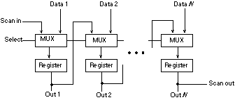
Figure 3.3.1 A register array showing the Scan In, Scan Out, and Select signals of the scan path.
Design for test (DFT) facilitates economical device testing. Complex VLSI devices without specific testability features can be prohibitively expensive to test to high-reliability requirements. Therefore, specific design approaches have evolved to make devices more readily testable.
All DFT approaches entail making trade-offs. For instance, many approaches require extra chip area or gates. Some techniques require additional device fabrication steps. The essential trade-off in DFT work occurs between the test circuitry costs, and test development and execution costs.
In this guide we focus on stuck-at fault testing. "Stuck-at" refers to a condition where a defect causes a circuit node to become "stuck" at a logical one or logical zero. A wide segment of the VLSI industry has adopted this testing approach because it can effectively create tests for large, modern VLSI designs with moderate present-day workstation computing power. Many tools have been marketed that support both the automatic generation of stuck-at fault test circuitry and the automatic generation of stuck-at fault tests (often called "stuck-at fault vectors"). These methods reduce the engineering time required for test generation. For more information on fault models, see "ASIC Designer Developed Tests" in Section Four, Chapter l.
In addition to stuck-at fault tests, designers must develop tests to show that the device's functions and parametric performances match the functional requirements of the device.
Stuck-at fault tests help to show that a design's logic circuit is accurately represented in every manufactured part, and that a manufacturing defect has not caused a distortion in a particular part's logic structure. CAD tools can usually automatically generate stuck-at fault tests. The tools generate these tests through a basic analysis of a design's structure, regardless of the functions the structure is meant to deliver. This narrow focus means stuck-at fault tests have little ability to test for intended function and performance.
For example, stuck-at fault tests can ensure that a counter has eight registers electrically wired according to the schematic. However, they have no ability to test that the original schematic properly described a circuit that would propagate an overflow when its count reached 64K. Tests to accomplish this are called functional tests and, at present, CAD tools cannot automatically generate them.
ASIC DFT has evolved around two major ASIC areas, I/O tests and internal tests. I/O tests involve an ASIC device's input and output pins. Internal tests focus on the device's core logic.
Many I/O tests are based on a technique known as "scan design." Scan design uses latches or flip-flops configured into a serial shift-register chain to pass test signals around a device and pass responses back to the outside world for analysis.
Scan design aims to achieve total or near total controllability and observability in sequential circuits. In this approach engineers design the ASIC flip-flops, latches, or both, to operate either in parallel (normal) mode or serial (test) mode. In the normal or system mode, the flip-flops and latches are configured for parallel operation. In test mode, the flip-flops and latches are loaded (controlled) by serially clocking in the desired data. In a similar fashion, engineers observe the data present in the flip-flops, latches, or both, by clocking out their contents in the serial test mode.
The basic element in scan design is a multiplexer placed ahead of each flip-flop, which is controlled for normal or test operation. (See Figure 3.3.1).
Figure 3.3.1 A register array showing the Scan In, Scan Out, and
Select signals of the scan path.
The multiplexer switches data between a scan in test signal and data, representing normal or system information. A select control line controls the switching. On the first scan design cell, the serial input connects to the primary input pin (Scan in). On intermediate cells, the serial input comes from the previous cell's output (Out signal). On the last cell, the output (Out N) connects to the primary output pin (Scan out signal). Selecting the test or serial mode creates a complete serial shift path from input pin to output pin.
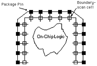
Boundary scan design extends the scan design idea to a board (system) or an ASIC level. This technique solves problems resulting from the combined effects of rising test equipment costs and difficulties in dealing with surface-mount technology. The technique places a boundary scan cell next to each component pin, as shown in Figure 3.3.2. Combined with scan design, as described above, boundary scan cells allow engineers to control and observe signals between chips. Besides their connections to the package pins and the internal chip logic, the boundary-scan cells have other terminals through which they can be connected to each other, forming a shift-register path around the periphery of the ASIC.
During normal operation, data passes between pins and internal chip logic as if the boundary-scan cells were not there. When put into the test mode, however, the test program directs data to pass along the shift register path. By loading data into the boundary-scan cells, the boundary-scan cells can inhibit data flow to or from the I/O pins, so that engineers can test either the internal logic or the external chip-to-chip connections.
The access to these component pins provides unique advantages to the test engineer. Using a shift path, arbitrary values can be loaded into the flip-flops and data can be extracted from those flip-flops. This enormously simplifies the pattern generation required to create tests for the ASIC logic.
IEEE Standard 1149.1 defines four pins and an optional fifth pin above and beyond the normal ASIC pins. These pins may drive the boundary-scan cells or special test logic on the ASIC, defined as a test access port (TAP). The standard also defines the TAP.
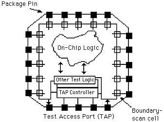
Figure 3.3.3 ASIC Structure Implementing the 1149.1 IEEE
Standard
Basically the TAP is a diagnostic socket on the ASIC, allowing external test equipment to control and communicate with the boundary-scan cells. Figure 3.3.3 illustrates in block diagram form the structure of the ASIC with the additional hardware required to implement the ANSI/IEEE standard.
Of the TAP pins, two provide for the serial data input and output [test data in (TDI), and test data out (TDO)]; the others control the data movement according to a defined protocol. A state machine (the TAP controller) interprets this protocol. This TAP controller generates the control signals required to operate the test tools built into the ASIC.
Designers can configure the ASIC TAP controller in a number of ways. Figure 3.3.3 shows a configuration providing a single daisy- chain serial data path that snakes its way around the ASIC device.
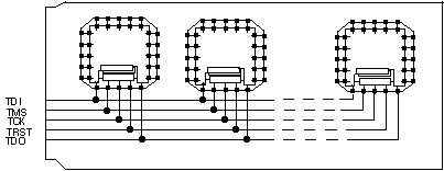
Figure 3.3.4 Boundary Scan applied to Multiple ASIC Devices
Since the IEEE standard provides for board testing, it may also be used for multiple ASIC testing. Figure 3.3.4, which shows the five extra TAP signals (TDI, TCK, TMS, TRST, and TDO) feeding multiple ASIC chips, illustrates this point.
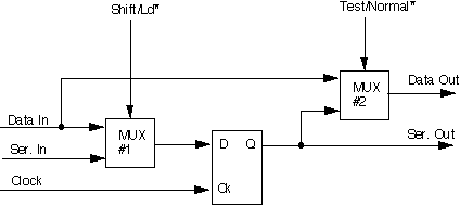
Figure 3.3.5 shows a block diagram of a boundary scan cell. Multiplexer number 1 (MUX number 1) provides for switching between normal data (Data In) and test data (Ser. In) via a Shift/Ld* control signal. This signal originates with the TAP controller. Multiplexer number 2 (MUX number 2) allows the user to bypass the boundary scan entirely by feeding Data In to Data Out via a Test/Normal* control signal from the TAP controller. Alternately it allows the test data (Q output of the D flip-flop) to feed the system (Data Out).
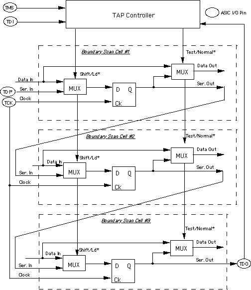
Figure 3.3.6 Boundary Scan Configuration
Figure 3.3.6 illustrates a simple boundary scan system providing a serial chain from Input to Output. This is implemented as follows:
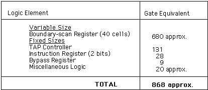
Table 3.3.1
Gate requirements for a Gate Array Boundary-scan Design
Note: In Table 3.3.1 the boundary-scan implementation requires 868 gates, requiring an estimated 8 percent overhead. Also note that the cells used in this example were created prior to publication of the IEEE 1149.1 standard. If specific cell designs had been available to support the standard or if the vendor had placed the boundary-scan circuitry in areas of the ASIC not available to the user, then the design would have required less.
We have presented and discussed the boundary scan's principle benefits and penalties. Careful planning and appropriate design tools can minimize the boundary scan costs. Test generation automated tools provide a major benefit when using boundary scan. The benefits of using boundary-scan also accrue during various testing stages. In each of these stages, boundary scan makes testing much more efficient by providing a standard, compact and efficient way to inject tests and observe their results. This feature becomes significant when field support and system maintenance represent key requirements. When viewed against the escalating costs of traditional functional or in-circuit test techniques for ASIC's, boundary-scan has attractive advantages.
LSSD imposes constraints on circuit excitation, particularly in handling clocked circuitry. Using this technique provides a circuit immune to most anomalies in the clock's AC characteristics.
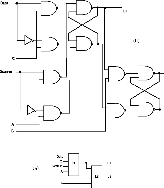
Figure 3.3.7 An LSSD Cell
In the LSSD environment, latches occur in pairs called shift register latches (SRLs) shown in Figure 3.3.7. Figure 3.3.7 (a) illustrates an LSSD cell block diagram, and Figure 3.3.7 (b) shows the LSSD cell's gate level schematic.
Multiple clocks A, B, and C control the latches. In normal operating mode, clock C clocks data into L1 from the data input and clock A is inactive. In the Scan (or testing) mode, clock A clocks in the scan data in, while clock C is inactive. Clock B transfers this data from L1 to L2. Output data can be taken from either L1 or L2.
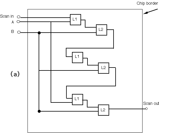
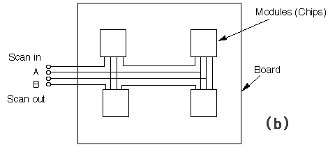
Figure 3.3.8 Application of LSSD Logic
Figure 3.3.8 (a) illustrates the threading concepts from the scan in signal to the scan out signal on an ASIC for shift register action using three LSSD cells. Figure 3.3.8 (b) applies the LSSD concept to four ASIC chips. Note that in Figure 3.3.8 the normal system clock, clock C, is not shown.
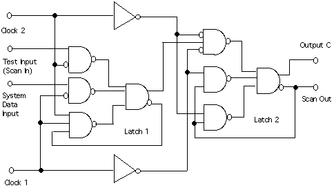
Figure 3.3.9 A Data Latch with Scan Path
Figure 3.3.9 shows the memory elements used in the scan path approach, referred to as raceless D type flip flops (Latch 1 and Latch 2).
In normal (or system) operation, Clock 2 is at logical 1 value for the entire operation thus blocking the Test Input for scan (test) mode. Clock 1 clocks the data into Latch 1 and 2.
In scan mode, Clock 1 is at logical 1 for the entire operation thus blocking the System data Input from normal mode. Clock 2 clocks the data into Latch 1 and 2.
This points out one of the significant differences between scan path and LSSD: latch clocking. The scan path technique utilizes clock signals (Clock 1 and Clock 2), thus providing an edge sensitive attribute rather than LSSD's level sensitive attribute.
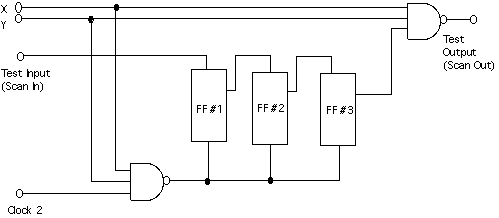
Figure 3.3.10 ASIC Configuration of Internal Devices in a Scan Path
Another scan path feature is the system configuration used in an ASIC. Figure 3.3.10, illustrates this with modules connected up in a serial scan path.
This configuration provides gates for selecting a particular scan path. In Figure 3.3.10, when X and Y are logical 1, clock 2, will be allowed to shift data through the scan path. At any other time, clock 2 and its output will be blocked.
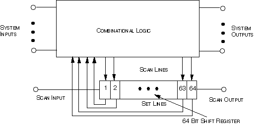
Scan /set logic, set forth by Sperry Univac uses principles similar to LSSD and scan path. Scan set logic, unlike scan path and LSSD, uses shift registers independent of all system data paths and latches. Figure 3.3.11 illustrates the Sperry Univac approach referred to as "bit serial logic."
In scan path and LSSD, you will recall that the shift registers were implemented in the data path. Figure 3.3.11 illustrates how the system sequential logic (the ASIC core logic) can be sampled for N points where N is the length of the external serial shift register. For Figure 3.3.11, N = 64. Upon loading the N points, a shifting process can occur, and the data can be scanned out through the Scan Output pin. This system also supports a set mode. In this mode, the Scan Input signal funnels data into the N bit serial shift register via the Scan Input signal and then appropriate clocking logic loads this data into the ASIC core system latches as required.
These internal tests aim to partition sequential networks into combinational networks for ease in testing. For the scan/set technique, the test pattern must set all latches in order to transform each partition under test to a combinational network.
This technique allows the scan function to occur during normal system operation--that is, the N bit serial shift register sampling pulse can occur while system clocks drive the ASIC sequential core logic. This allows diagnosing the sequential machine without degrading system performance.
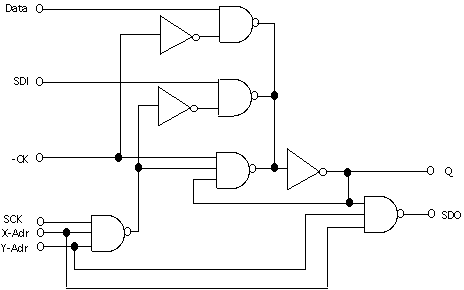
Figure 3.3.12 Random-Acess Scan Cell
Figure 3.3.12 shows one implementation of a random-access scan cell.
This cell has a single latch with an extra data port added [scan data in (SDI) port]. SCK clocks test data into the latch. The SCK clock can only affect the latch when both X and Y are logically 1. Additionally the output, Serial Data Out (SDO) is active only when both X and Y are logically 1.
In the normal (system) mode the system clock, CK, loads data into the latch.
Engineers have used scan cell configurations, other than this one, to implement this technique. However, they will not be discussed.
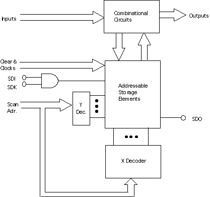
Figure 3.3.13 Random-Acess Scan System
Figure 3.3.13 gives a system perspective of the random-access scan technique.
Figure 3.3.13 illustrates Clear, Clocks, SDI, SDK, Scan Address, and SDO test signals. SDI scans data in for the addressed latch, and SDO scans data out for the addressed latch. The test hardware comprises an X and a Y Decoder and the addressable storage elements (the random- access scan cells).
The random-access scan technique provides observability at any point in the combinational network.
The random-access scan approach requires about three to four gates per storage element compared to two latches for every point in the scan path approach or the LSSD approach. Implementing this approach requires 10 to 20 I/O pins. Engineers can reduce this pin overhead by using a serial approach for the scan address, which leads to a six pin I/O overhead.
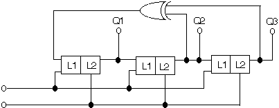
Figure 3.3.14 An Example Linear Feedback Shift Regular
A linear-feedback shift register (LFSR) provides the foundation for signature analysis. Figure 3.3.14 gives an example of a three-bit LFSR.
The LFSR in figure 3.3.14 uses three SRLs with an Exclusive Or feedback. Inputs to the Exclusive Or circuit, called "TAPS," come from shift register chain outputs (Q2 and Q3 for this example). Designers best design these shift register TAPS and the resulting test patterns by consulting tables. Engineers often call the test patterns pseudo random patterns.
Designers can set up an LFSR to send output serially (through Q3 in figure 3.3.14) or in parallel (Q1, Q2, and Q3 in figure 3.3.14). These outputs become the test inputs for the BILBO logic and allow a network to test itself.
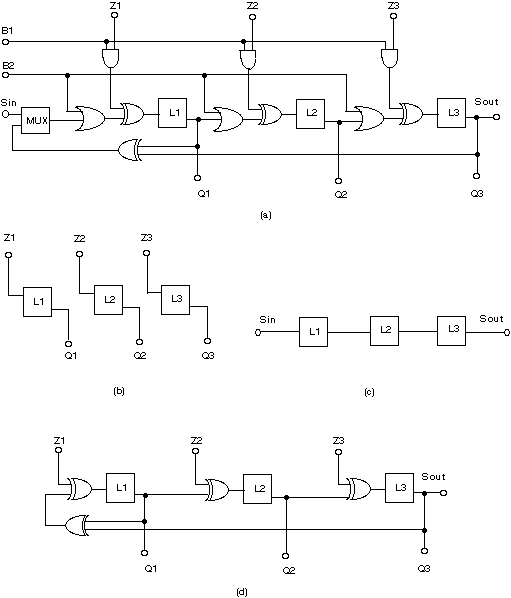
Figure 3.3.15 BILBO and its Operating Modes
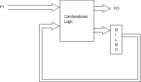
Figure 3.3.16 presents a block diagram of the BILBO structure. This structure is basically a latch (L1, L2, or L3) fed by combinational logic. In a system operating mode this can be thought of as inputs (Z1, Z2, and Z3 ) coming from a combinational logic block (from the ASIC) with outputs (Q1, Q2, and Q3) connecting to another combinational logic block within the ASIC. This BILBO functions in three operating modes. (See Table 3.3.2). P1 and PO comprise the primary I/O for the ASIC chip. The ASIC feeds its outputs to the BILBO for testing, while the BILBO sends test results back to the ASIC's combinational logic.
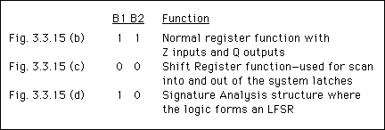
Table 3.3.2 BILBO Functions
Below we briefly discuss some of the advantages and disadvantages of this technique.
FDL proposes a fault dictionary format standard so that engineers can pass fault dictionary data between CAD tools. The dictionary format standard would also aid stuck-at fault test standardization between chips, boards, and systems.
Using a fault dictionary results in two major benefits:
WAVES describes a language for generating the inputs and capturing the outputs of digital electronic circuit simulations. WAVES support all circuit model levels, except for the lowest analog transistor levels where designers normally use SPICE simulations.
The stimuli (inputs) and responses (outputs) that WAVES supports can be transferred to other CAD tools for system simulations or to testers for device testing.
TRSL proposes a standard for specifying digital electronics electrical test requirements. A TRSL test specification would, for example, allow:
At a higher level, TRSL provides test-intent documentation. Therefore, ASIC vendor test engineers who find a problem with a detailed test, can go back to the TRSL intent for that test and perhaps satisfy it with another detailed test approach.
ANSI/IEEE Standard 1149.1-1990, IEEE Standard Test Access Port and Boundary-Scan Architecture, IEEE Standards Board, New York, N.Y, May 1990.
S. Das Gupta, et al, "Chip partitioning aid: a design technique for partitionability and testability in VLSI," ACM/IEEE Design Automation Conference Proceedings, IEEE Computer Society Press, Los Alamitos, CA, 1984, pp. 203-208.
S. DasGupta, E.B. Eichelberger, and T.W. Williams, "LSI chip design for testability," Dig. 1978 Int. Solid-State Conf., San Francisco, CA, Feb. 1978, pp. 216-217.
E.B. Eichelberger and T.W. Williams, "A logic design structure for LSI testability," J. Design Automat. Fault-Tolerant Comput., vol. 2, May 1978, pp. 165-1789.
_____, "A logic design structure for LSI testing," Proc. 14th Des. Automat. Conf., June 1977, 77CH1216-1C, pp. 462- 468.
E.B. Eichelberger, E.J. Muehldoref, R.G. Walter, and T.W. Williams, "A logic design structure for testing internal arrays," Proc. 3rd USA-Japan Comput. Conf., San Francisco, CA, Oct. 1978, pp. 266-272.
R.A. Frohwerk, "Signature analysis: A new digital field service method," Hewlett-Packard J., May 1977 pp. 2-8.
S. Funatsu, N. Sakatsuki, and T. Arima, "Test generation systems in Japan," Proc. 12th Des. Automat. Symp., June 1975, pp. 114-122.
IEEE, "Testability on TAP," IEEE Spectrum, February, 1992, pp. 34-37.
LSI Logic Corp., CMOS macrocell manual, LSI Logic Corp., Milpitas, CA, Sept. 1984.
B. Koenemann, J. Mucha, and G. Zwichoff, "Built-in logic block observation techniques," Dig. 1979 Test Conf., Oct. 1979, 79CH1509-9C, pp. 37-41.
C.M. Maunder and R.E. Tulloss: The test access port and boundary- scan architecture, IEEE Computer Society Press, Los Alamitos, CA, 1990.
_____, "Benefits and penalties of boundary scan," The Test Access Port and Boundary-Scan Architecture, IEEE Computer Society Press, Los Alamitos, CA, 1990.
H.J. Nadig, "Signature analysis - Concepts, examples, and guidelines," Hewlett-Packard J., May 1977, pp. 15-21.
W.W. Peterson and E.J. Weldon, Error correcting codes, MIT Press, Cambridge MA, 1972.
J.H. Stewart, "Future testing of large LSI circuit cards," Dig. 1977 Semiconductor Test Symp., 77CH1261-7C, Oct. 1977, pp. 6-17.
M.J.Y. Williams and J.B. Angell, "Enhancing testability of large scale integrated circuits via test points and additional logic," IEEE Trans. Comput., vol. C-22, Jan. 1973, pp. 46-60.
E. White, "Signature analysis, enhancing the serviceability of micro-processor-based industrial products," Proc. 4th IECI Annu. Conf., 78CH1312-8, Mar. 1978, pp. 68-76.
T.W. Williams, "Utilization of a structured design for reliability & serviceability," Dig. Government Microcircuits Applications Conf., Monterey, CA., Nov. 1978, pp. 441-444.
_____, "Design for testability - a survey," IEEE Transactions on Computers, Vol. C-31, No.1, Jan. 1982.
Now you may jump to: